 | ÐлекÑÑоннÑй компоненÑ: IRSF3021L | СкаÑаÑÑ:  PDF PDF  ZIP ZIP |
/home/web/doc/html/irf/174997

Data Sheet No. PD 60068-
I
Description
The IRSF3021 Lamp and DC motor driver is a fully protected
three terminal monolithic Smart Power MOSFET that fea-
tures current limiting, over-temperature protection, ESD
protection and over-voltage protection.
The on-chip protection circuit limits the drain current at 5.5A
(typical) in the on-state, when the load is short circuited. The
over-temperature circuitry turns off the Power MOSFET when
the junction temperature exceeds 165°C (typical). The device
restarts automatically once it has cooled down below the reset
temperature.
The IRSF3021 is specifically designed for driving loads that
require overload protection and in-rush current control while
operating in automotive and industrial environments. Tar-
geted applications include resistive loads such as lamps or
capacitive loads such as airbag squibs and DC motor drives.
FULLY PROTECTED POWER MOSFET SWITCH
Features
·
Controlled slew rate reduces EMI
·
Over temperature protection with auto-restart
·
Linear current-limit protection
·
Active drain-to-source clamp
·
ESD protection
·
Lead compatible with standard Power MOSFET
·
Low operating input current
·
Monolithic construction
Applications
·
Cabin Lighting
·
Airbag System
·
Programmable Logic Controller
·
DC Motor Drive
IRSF3021
(NOTE: For new designs, we
recommend IR's new products IPS021 and IPS021L)
Product Summary
Source
SOURCE
V
ds(clamp)
50V
R
ds(on)
200m
I
lim
5.5A
T
j(sd)
165
o
C
E
AS
200mJ
Packages
3 Lead
TO220AB
3 Lead
SOT223
www.irf.com
1
Block Diagram
Drain
Input
DRAIN
INPUT
IRSF3021
2
www.irf.com
N
OTES
:
x
When mounted on a 1" square PCB (FR-4 or G10 material). For recommended footprint and soldering techniques,
refer to International Rectifier Application Note AN-994.
y
E
AS
is tested with a constant current source of 6A applied for 700µS with V
in
= 0V and starting T
j
= 25oC.
z
Input current must be limited to less than 5mA with a 1k
resistor in series with the input when the Body-Drain Diode is
forward biased.
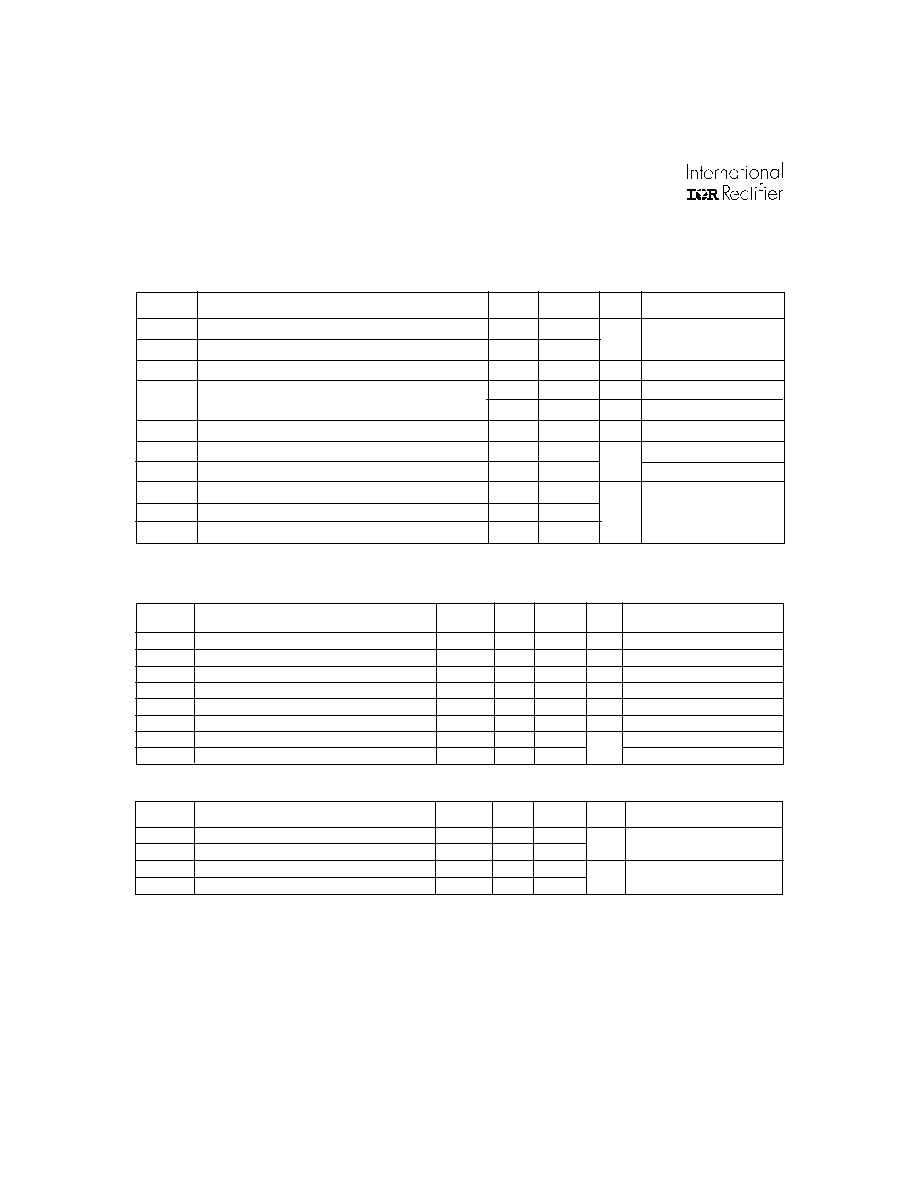
Symbol Parameter
Min.
Typ.
Max. Units Test Conditions
R
thjc
Junction to case
--
--
4
o
C/W TO-220AB
R
thja
Junction to ambient
--
--
60
R
thjc
Junction to case
--
--
40
o
C/W SOT-223
R
thja
Junction to PCB
--
--
60
Thermal Characteristics
Symbol Parameter
Min.
Typ.
Max. Units Test Conditions
V
ds,clamp
Drain to source clamp voltage
50
56
65
V
I
ds
= 6A, t
p
= 700
µ
S
R
ds(on)
Drain to source on resistance
--
155
200
m
V
in
= 5V, I
ds
= 2A
I
dss
Drain to source leakage current
--
--
250
µ
A
V
ds
= 40V, V
in
= 0V
V
th
Input threshold voltage
1.0
2.0
3.0
V
V
ds
= V
in
, I
ds
+ I
in
= 10mA
I
i,on
Input supply current
(Normal Operation)
--
100
300
µ
A
V
in
= 5V
I
i,off
Input supply current
(Protection Mode)
--
250
500
µ
A
V
in
= 5V
V
in, clamp
Input clamp voltage
9
10
--
I
in
= 1mA
V
sd
Body-drain diode forward drop
--
1.5
--
I
ds
= -2A, R
in
= 1k
Static Electrical Characteristics
(T
C
= 25
o
C unless otherwise specified.)
V
Absolute Maximum Ratings
Absolute Maximum Ratings indicate sustained limits beyond which damage to the device may occur.
(T
C
= 25
o
C unless otherwise specified.)
Symbol Parameter
Min.
Max.
Units
Test Conditions
Vds, max Continuous drain to source voltage
--
50
V
Vin, max Continuous input voltage
-0.3
10
Ids
Continuous drain current
--
self limited
A
Pd
Power dissipation
--
30
W
Tc
25
o
C, TO220
--
3
W
Tc
25
o
C, SOT223
EAS
Unclamped single pulse inductive energy
Á
--
200
mJ
Vesd1
Electrostatic discharge voltage
(Human Body Model)
--
4000
V
100pF, 1.5k
Vesd2
Electrostatic discharge voltage
(Machine Model)
--
1000
200pF, 0
TJop
Operating junction temperature range
-55
150
TStg
Storage temperature range
-55
150
o
C
TL
Lead temperature (soldering, 10 seconds)
--
300

IRSF3021
www.irf.com
3
Switching ElectricalCharacteristics
(V
CC
= 14V, resistive load (R
L
) = 10
,
R
in
= 100
.
Specifications measured at T
C
= 25oC unless other-
wise specified.)
Symbol Parameter
Min.
Typ.
Max. Units Test Conditions
t
don
Turn-on delay time
--
10
50
V
in
= 0V to 5V, 50% to 90%
t
r
Rise Time
--
30
80
µ
s
V
in
= 0V to 5V, 90% to 10%
t
doff
Turn-off delay time
--
20
60
V
in
= 5V to 0V, 50% to 10%
t
f
Fall time
--
15
50
V
in
= 5V to 0V, 10% to 90%
SR
Output positive slew rate
-4
--
4
V/
µ
s
V
in
= 0V to 5V, +dVds/dt
SR
Output negative slew rate
-4
--
4
V
in
= 5V to 0V, -dVds/dt
Protection Characteristics
(T
C
= 25
o
C unless otherwise specified.
Symbol Parameter
Min.
Typ.
Max. Units Test Conditions
I
ds(lim)
Current limit
3.0
5.5
8.0
A
Vin = 5V, Vds
= 14V
T
j(sd)
Over temperature shutdown threshold
155
165
--
o
C
Vin = 5V, Ids = 2A
V
protect
Min. input voltage for over-temp function
--
3
--
V
t
Iresp
Current limit response time
--
TBD
--
µ
s
I
peak
Peak short circuit current
--
10
--
A
t
Tresp
Over-temperature response time
--
TBD
--
µ
s
Lead Assignments
Part Number
(2) D
1 2 3
In D S
3 Lead - SOT223
IRSF3021L
1 2 3
In D S
3 Lead - TO220
2 (D)
IRSF3021

IRSF3021
4
www.irf.com
(TO-261AA) 01-0022 05
Case Outline - SOT-223

IRSF3021
www.irf.com
5
IR WORLD HEADQUARTERS: 233 Kansas St., El Segundo, California 90245 Tel: (310) 252-7105
IR EUROPEAN REGIONAL CENTRE: 439/445 Godstone Rd, Whyteleafe, Surrey CR3 0BL, United Kingdom
Tel: ++44 (0) 20 8645 8000
IR JAPAN: K&H Bldg., 2F, 30-4 Nishi-Ikebukuro 3-Chome, Toshima-Ku, Tokyo, Japan 171-0021 Tel: 81 (0) 33 983 0086
IR HONG KONG: Unit 308, #F, New East Ocean Centre, No. 9 Science Museum Road, Tsimshatsui East, Kowloon,
Hong Kong Tel: (852) 2803-7380
Data and specifications subject to change without notice. 4/11/2000
Tape & Reel - SOT223
01-0028 05 / 01-0008 02
IRGB 01-3026 01
Case Outline 3 Lead - TO220
NOTES:
2
2X