IRU1260
1
Rev. 2.1
09/19/02
www.irf.com
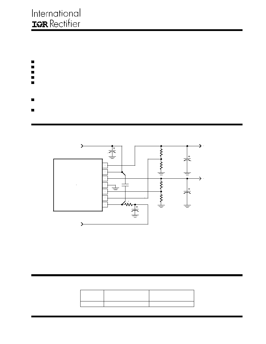
TYPICAL APPLICATION
DESCRIPTION
The IRU1260 uses a proprietary process and combines
a dual low dropout adjustable output regulator in a single
package with one output having a minimum of 6A and
the other one having a 1A output current capability. This
product is specifically designed to provide well regulated
supplies for low voltage ICs such as 3.3V to 1.5V and
2.5V supplies for the GTL+ termination and the new
clock for Pentium
II
TM
applications. Other applications
include low cost dual supply for processors such as Intel
P55C
TM
where 2.8V and 3.3V are needed for the Core
and the I/O supplies from the 5V input.
DUAL 6A AND 1A LOW DROPOUT
POSITIVE ADJUSTABLE REGULATOR
Figure 1 - Typical application of IRU1260 in the Pentium
II
TM
design with the 1.5V output
providing for GTL+ termination while 2.5V supplies the clock chip.
Notes: Pentium
II
TM
is trademark of Intel Corp.
P55C
TM
is trademark of Intel Corp.
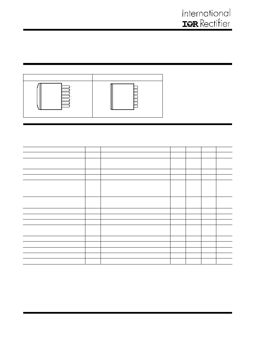
PACKAGE ORDER INFORMATION
T
J
(
�
C) 7-PIN PLASTIC 7-PIN PLASTIC
TO-263 (M) Ultra Thin-Pak
TM
(P)
0 To 150 IRU1260CM IRU1260CP
Data Sheet No. PD94138
FEATURES
Providing a Single Package Solution for GTL+ and
High Speed Bus Termination
Dual Supply P55C
TM
Applications
APPLICATIONS
Guaranteed <1.3V Dropout at 6A (Output #2)
Guaranteed <0.6V Dropout at 1A (Output #1)
Fast Transient Response
1% Voltage Reference Initial Accuracy
Built-In Thermal Shutdown
3.3V
2.5V / 1A
1.5V / 6A
C1
R1
R2
R3
R4
C2
C3
IRU1260
5V
C5
U1
C4
R5
V
CTRL
V
FB
1
V
FB
2
Gnd
V
OUT
2
V
IN
V
OUT
1
1
2
3
4
5
6
7
IRU1260
2
Rev. 2.1
09/19/02
www.irf.com
V
CTRL
Input Voltage
Reference Voltage
Line Regulation
Load Regulation (Note 1)
Dropout Voltage (Output #2)
(Note 2)
Dropout Voltage (Output #1)
(Note 2)
Current Limit (Output #2)
Current Limit (Output #1)
Thermal Regulation
Ripple Rejection
Feedback Pin Input Current
Temperature Stability
Long Term Stability
RMS Output Noise
Minimum Load Current (Note 3)
ABSOLUTE MAXIMUM RATINGS
Input Voltage (V
IN
) .................................................... 7V
Power Dissipation ..................................................... Internally Limited
Storage Temperature Range ...................................... -65�C To 150�C
Operating Junction Temperature Range ..................... 0�C To 150�C
PACKAGE INFORMATION
7-PIN PLASTIC TO-263 (M) 7-PIN ULTRA THIN-PAK (P)
JA
=30
8
C/W for 1"sq pad
JA
=30
8
C/W for 1"sq pad
ELECTRICAL SPECIFICATIONS
Unless otherwise specified, these specifications apply over C
IN
=1
m
F, C
OUT
=10
m
F and T
J
=0 to 150�C. Typical values
refer to T
J
=25
�
C. I
FL
=6A for output #1 and I
FL
=1A for output #2. V
FB
=V
OUT
for both outputs. V
CTRL
=V
IN
=3.3V.
Note 3: Minimum load current is defined as the mini-
mum current required at the output in order for the out-
put voltage to maintain regulation. Typically the resistor
divider values are selected such that this current is au-
tomatically maintained.
Note 1: Low duty cycle pulse testing with Kelvin con-
nections is required in order to maintain accurate data.
Note 2: Dropout voltage is defined as the minimum dif-
ferential voltage between V
IN
and V
OUT
required to main-
tain regulation at V
OUT
. It is measured when the output
voltage drops 1% below its nominal value.
PARAMETER
SYM TEST CONDITION MIN TYP MAX UNITS
Io=10mA, T
J
=25�C
Io=10mA
Io=10mA, V
OUT
+1.3V<V
IN
=V
CTRL
<7V
10mA<Io<I
FL
Io=4A, V
CTRL
=4.75V, V
IN
=3.3V
Io=3A, V
CTRL
=4.75V, V
IN
=3.3V
Io=2A, V
CTRL
=4.75V, V
IN
=3.3V
Io=1A, V
CTRL
=4.75V, V
IN
=3.3V
Io=1A, V
CTRL
=V
IN
=4.75V
D
Vo=100mV
D
Vo=100mV
30ms pulse, Io=I
FL
f=120Hz, Co=25
m
F Tantalum,
Io=0.5
3
I
FL
Io=10mA
Io=10mA
T
A
=125�C, 1000Hrs
T
A
=25�C, 10Hz<f<10KHz
3.0
1.188
1.176
6.1
1.1
V
V
%
%
V
V
A
A
%/W
dB
m
A
%
%
%V
O
mA
1.212
1.224
1.0
0.7
0.5
0.6
1.3
0.02
1
1.200
1.200
0.2
0.4
0.35
0.4
0.01
70
0.02
0.5
0.3
0.003
5
V
REF
I
CL2
I
CL1
I
FB
V
CTRL
V
FB
1
V
FB
2
Gnd
V
OUT
2
V
IN
V
OUT
1
1
2
3
4
5
6
7
1
2
3
4
5
6
7
V
CTRL
V
FB
1
V
FB
2
Gnd
V
OUT
2
V
IN
V
OUT
1
IRU1260
3
Rev. 2.1
09/19/02
www.irf.com
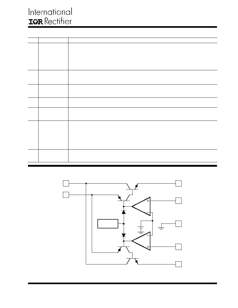
BLOCK DIAGRAM
Figure 2 - Simplified block diagram of the IRU1260.
The control input pin of the regulator. This pin via a 10
V
resistor is connected to the 5V
supply to provide the base current for the pass transistor of both regulators. This allows
the regulator to have very low dropout voltage which allows one to generate a well regu-
lated 2.5V supply from the 3.3V input. A high frequency, 1
m
F capacitor is connected
between this pin and V
IN
pin to insure stability.
A resistor divider from this pin to V
OUT
1 pin and ground sets the output voltage. See
application circuit for the divider setting for 2.5V output.
A resistor divider from this pin to the V
OUT
2 pin and ground sets the output voltage. See
application circuit for the divider setting for 1.5V output.
This pin is connected to ground. It is also the tab of the package.
The output #2 (high current) of the regulator. A minimum of 100
m
F capacitor must be
connected from this pin to ground to insure stability.
The power input pin of the regulator. Typically a large storage capacitor is connected from
this pin to ground to insure that the input voltage does not sag below the minimum dropout
voltage during the load transient response. This pin must always be higher than both V
OUT
pins by the amount of the dropout voltage in order for the device to regulate properly.(See
data sheet)
The output #1 (low current) of the regulator. A minimum of 100
m
F capacitor must be
connected from this pin to ground to insure stability.
PIN # PIN SYMBOL
PIN DESCRIPTION
PIN DESCRIPTIONS
1
2
3
4
5
6
7
V
CTRL
V
FB
1
V
FB
2
Gnd
V
OUT
2
V
IN
V
OUT
1
V
CTRL
V
IN
Gnd
6
1
4
5 V
OUT
2
7 V
OUT
1
THERMAL
SHUTDOWN
1.20V
2 V
FB
1
3 V
FB
2
+

IRU1260
4
Rev. 2.1
09/19/02
www.irf.com
Introduction
The IRU1260 is a dual adjustable Low Dropout (LDO)
regulator which can easily be programmed with the ad-
dition of two external resistors to any voltages within
the range of 1.20 to 5.5V. This voltage regulator is de-
signed specifically for applications that require two sepa-
rate regulators such as the Intel Pentium
II
TM
proces-
sors requiring 1.5V and 2.5V supplies, eliminating the
need for a second regulator which results in lower over-
all system cost. When V
CTRL
pin is connected to a sup-
ply which is at least 1V higher than V
IN
, the dropout
voltage improves by 30% which makes it ideal for appli-
cations requiring less than the standard 1.3V dropout
given in the LDO products such as IRU10XX series. The
IRU1260 also provides an accurate 1.20V voltage refer-
ence common to both regulators for programming each
output voltage. Other features of the device include: fast
response to sudden load current changes, such as GTL+
termination application for Pentium
II
TM
family of micro-
processors. The IRU1260 also includes thermal shut-
down protection to protect the device if an overload con-
dition occurs.
Output Voltage Setting
The IRU1260 can be programmed to any voltages in the
range of 1.20V to 5.5V with the addition of R1 and R2
external resistors according to the following formula:
Figure 3 - Typical application of the IRU1260
for programming the output voltage.
(Only one output is shown here)
V
OUT
R2
R1
V
IN
V
CTRL
V
REF
I
B
IRU1260
Gnd
V
OUT
V
CTRL
V
IN
V
FB
R 2
R 1
V
I N
V
C T R L
R
L
R
P
PARASITIC LINE
RESISTANCE
IRU1260
Gnd
V
OUT
V
CTRL
V
IN
V
FB
Where:
V
REF
= 1.20V Typically
I
B
= 0.02
m
A Typical
R1 and R2 as shown in Figure 3:
V
OUT
= V
REF
3
+R
2
3
I
B
R
2
R
1
(
)
1+
The IRU1260 keeps a constant 1.2V between the V
FB
pin and ground pin. By placing a resistor R1 across these
two pins a constant current flows through R1, adding to
the I
FB
current and into the R2 resistor producing a volt-
age equal to the (1.2/R1)
3
R2 + I
FB
3
R2 which will be
added to the 1.2V to set the output voltage as shown in
the above equation. Since the input bias current of the
amplifier (I
FB
) is only 0.02
m
A typically, it adds a very
small error to the output voltage and for most applica-
tions can be ignored. For example, in a typical 1.5V
GTL+application if R1=10.2K
V
and R2=2.55K
V
the er-
ror due to the I
ADJ
is only 0.05mV which is less than
0.004% of the nominal set point. The effective input im-
pedance seen by the feedback pins (The parallel combi-
nation of R1 and R2) must always be higher than 1.8K
V
in order for the regulator to start up properly.
Load Regulation
Since the IRU1260 does not provide a separate ground
pin for the reference voltage, it is not possible to provide
true remote sensing of the output voltage at the load.
Figure 4 shows that the best load regulation is achieved
when the bottom side of R1 resistor is connected di-
rectly to the ground pin of IRU1260 (preferably to the tab
of the device) and the top side of R2 resistor is con-
nected to the load. In fact, if R1 is connected to the load
side, the effective resistance between the regulator and
the load is gained up by the factor of (1+R2/R1), or the
effective resistance will be, R
P(eff)
=R
P
3
(1+R2/R1). It is
important to note that for high current applications, this
can represent a significant percentage of the overall load
regulation and one must keep the path from the regula-
tor to the load as short as possible to minimize this
effect.
Figure 4 - Schematic showing connection
for best load regulation.
(Only one output is shown here)
APPLICATION INFORMATION
IRU1260
5
Rev. 2.1
09/19/02
www.irf.com
Stability
The IRU1260 requires the use of an output capacitor as
part of the frequency compensation in order to make the
regulator stable. Typical designs for the microprocessor
applications use standard electrolytic capacitors with
typical ESR in the range of 50 to 100m
V
and the output
capacitance of 500 to 1000
m
F. Fortunately as the ca-
pacitance increases, the ESR decreases resulting in a
fixed RC time constant. The IRU1260 takes advantage
of this phenomena in making the overall regulator loop
stable. For most applications a minimum of 100
m
F alu-
minum electrolytic capacitor with the maximum ESR of
0.3
V
such as Sanyo, MVGX series, Panasonic FA se-
ries as well as the Nichicon PL series insures both sta-
bility and good transient response. The IRU1260 also
requires a 1
m
F ceramic capacitor connected from V
IN
to
V
CTRL
and a 10
V
, 0.1W resistor in series with V
CTRL
pin
in order to further insure stability.
Thermal Design
The IRU1260 incorporates an internal thermal shutdown
that protects the device when the junction temperature
exceeds the maximum allowable junction temperature.
Although this device can operate with junction tempera-
tures in the range of 150
8
C, it is recommended that the
selected heat sink be chosen such that during maxi-
mum continuous load operation the junction tempera-
ture is kept below this number. The example given shows
the steps in selecting the proper regulator heat sink for
driving the Pentium
II
TM
processor GTL+ termination
resistors and the Clock IC using the IRU1260 TO-263
package.
Example:
Assuming the following specifications:
The steps for selecting a proper heat sink to keep the
junction temperature below 135
8
C is given as:
1) Calculate the maximum power dissipation using:
2) Assuming a TO-263 surface mount package, the junc-
tion to ambient thermal resistance of the package is:
3) The maximum junction temperature of the device is
calculated using the equation below:
Since this is lower than our selected 135
8
C maxi-
mum junction temperature (150
8
C is the thermal shut-
down of the device), TO-263 package is a suitable
package for our application.
V
IN
= 3.3V
V
OUT1
= 2.5V
V
OUT2
= 1.5V
I
OUT1(MAX)
= 0.2A
I
OUT2(MAX)
= 1.5A
T
A
= 35
8
C
P
D
= I
OUT1
3
(V
IN
- V
OUT1
) + I
OUT2
3
(V
IN
- V
OUT2
)
P
D
= 0.2
3
(3.3 - 2.5) + 1.5
3
(3.3 - 1.5) = 2.86W
u
JA
= 30
8
C/W for 1" square pad area
T
J
= T
A
+ P
D
3u
JA
T
J
= 35 + 2.86
3
30 = 121
8
C