
IRU3046
1
Rev. 1.9
09/27/02
www.irf.com
TYPICAL APPLICATION
DESCRIPTION
The IRU3046 IC combines a Dual synchronous Buck
controller and a linear regulator controller, providing a
cost-effective, high performance and flexible solution for
multi-output applications. The Dual synchronous con-
troller can be configured as 2-independent or 2-phase
controller. In 2-phase configuration, the IRU3046 provides
a programmable current sharing which is ideal when the
output power exceeds any single input power budget.
IRU3046 provides a separate adjustable output by driv-
ing a switch as a linear regulator. This device features
programmable switching frequency up to 400KHz per
phase, under-voltage lockout for all input supplies, an
external programmable soft-start function as well as out-
put under-voltage detection that latches off the device
when an output short is detected.
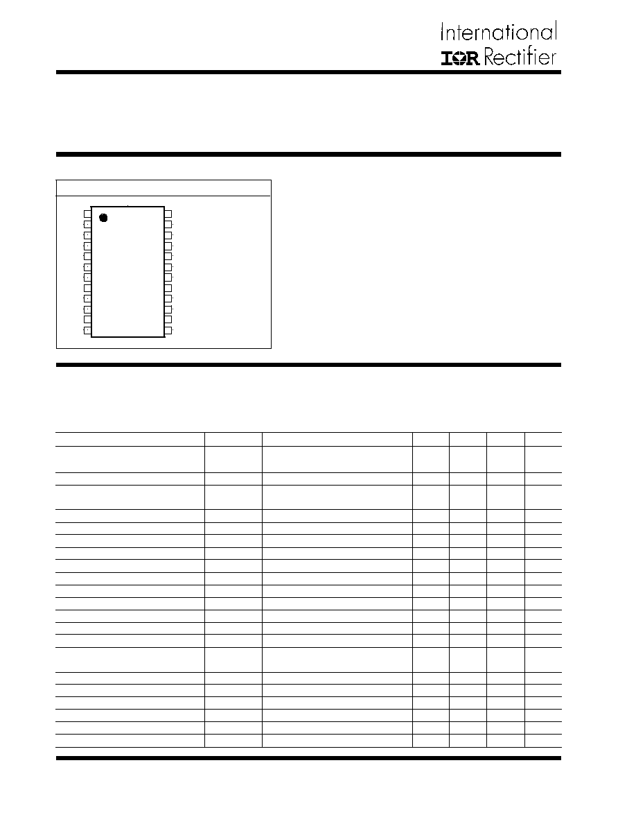
Dual Synchronous Controller in 24-Pin Package
with 180
8
out-of-phase operation
LDO Controller with Independent Bias Supply
Can be configured as 2-Independent or 2-Phase
PWM Controller
Programmable Current Sharing in 2-Phase Configu-
ration
Flexible, Same or Separate Supply Operation
Operation from 4V to 25V Input
Programmable Switching Frequency up to 400KHz
Soft-Start controls all outputs
Precision Reference Voltage Available
500mA Peak Output Drive Capability
Short Circuit Protection for all outputs
Power Good Output
Synchronizable with External Clock
FEATURES
DUAL SYNCHRONOUS PWM CONTROLLER WITH
CURRENT SHARING CIRCUITRY AND LDO CONTROLLER
APPLICATIONS
PRELIMINARY DATA SHEET
Data Sheet No. PD94251
Figure 1 - Typical application of IRU3046 configured as 2-phase converter with current sharing.
Dual-Phase Power Supply
DDR Memory Source Sink Vtt Application
Graphic Card
Hard Disk Drive
Power supplies requiring multiple outputs
PACKAGE ORDER INFORMATION
T
A
(�C) DEVICE PACKAGE FREQUENCY
0 To 70 IRU3046CF 24-Pin Plastic TSSOP (F) 200-400KHz
12V
5V
V
OUT2
PGood
C1
C2
L1
C6
R2
Q5
C18
R10
L4
Q4
Q1
C5
C7
3.3V
U1
V
OUT1
R8
C16
L3
C17
R5
R9
R7
C10
R1
R4
C9
R3
C8
C3
C4
C13
D1
D2
C11
PGnd
V
CL
V
OUT3
LDrv1
HDrv1
Fb1
Vp2
Fb2
LDrv2
HDrv2
VcH1
VcH2
Vcc
Gnd
Comp2
Fb3
Comp1
SS
PGood
V
REF
IRU3046
L2
C12
Q3
C15
R6
Q2
C14
Sync
Rt
V
SEN33
VccLDO
2
Rev. 1.9
09/27/02
IRU3046
www.irf.com
ELECTRICAL SPECIFICATIONS
Unless otherwise specified, these specifications apply over Vcc=5V, VcH1=VcH2=V
CL
=VccLDO=12V and T
A
=0 to
70�C. Typical values refer to T
A
=25�C. Low duty cycle pulse testing is used which keeps junction and case tem-
peratures equal to the ambient temperature.
ABSOLUTE MAXIMUM RATINGS
Vcc Supply Voltage .................................................. 25V
VccLDO, VcH1, VcH2 and V
CL
Supply Voltage ........... 30V (not rated for inductive load)
Storage Temperature Range ...................................... -65�C To 150�C
Operating Junction Temperature Range ..................... 0�C To 125�C
PACKAGE INFORMATION
24-PIN PLASTIC TSSOP (F)
PARAMETER
SYM TEST CONDITION
MIN TYP MAX UNITS
Reference Voltage Section
Fb Voltage
Fb Voltage Line Regulation
UVLO Section
UVLO Threshold - Vcc
UVLO Hysteresis - Vcc
UVLO Threshold - VccLDO
UVLO Hysteresis - VccLDO
UVLO Threshold - VcH1
UVLO Hysteresis - VcH1
UVLO Threshold - VcH2
UVLO Hysteresis - VcH2
UVLO Threshold - Fb
UVLO Hysteresis - Fb
UVLO Threshold - V
SEN33
UVLO Hysteresis - V
SEN33
Supply Current Section
Vcc Dynamic Supply Current
VcH1 Dynamic Supply Current
VcH2 Dynamic Supply Current
Vcc Static Supply Current
VcH1 Static Supply Current
VcH2 Static Supply Current
VccLDO Static Supply Current
5<Vcc<12
Supply Ramping Up
Supply Ramping Up
Supply Ramping Up
Supply Ramping Up
Fb Ramping Down
Supply Ramping Up
Freq=200KHz, C
L
=1500pF
Freq=200KHz, C
L
=1500pF
Freq=200KHz, C
L
=1500pF
SS=0V
SS=0V
SS=0V
SS=0V
1.225 1.250
0.2
4.2
0.25
4.2
0.25
3.5
0.2
3.5
0.2
0.6
0.1
2.5
0.2
5
7
7
3.5
2
2
1
1.275
V
%
V
V
V
V
V
V
V
V
V
V
V
V
mA
mA
mA
mA
mA
mA
mA
JA
= 84
�
C/W
Vcc
Comp1
Comp2
Rt
Sync
VcH2
HDrv2
LDrv2
Fb2
PGnd
V
CL
LDrv1
HDrv1
VcH1
VccLDO
V
OUT3
Fb3
SS
Fb1
V
SEN33
Vp2
PGood
V
REF
Gnd
4
3
2
1
21
22
23
24
7
6
5
18
19
20
TOP VIEW
12
13
11
14
10
15
9
16
8
17
V
FB
L
REG
UVLO
V
CC
UVLO
V
CC
LDO
UVLO
V
C
H1
UVLO
V
C
H2
UVLO
Fb
UVLO
V
SEN33
Dyn I
CC
Dyn I
C
H1
Dyn I
C
H2
I
CCQ
I
C
H1Q
I
C
H2Q
I
C
LDO
IRU3046
3
Rev. 1.9
09/27/02
www.irf.com
PARAMETER
SYM TEST CONDITION MIN TYP MAX UNITS
Soft-Start Section
Charge Current
Power Good Section
Fb1 Lower Trip Point
Fb1 Upper Trip Point
Fb2 Lower Trip Point
Fb2 Upper Trip Point
Fb3 Lower Trip Point
Fb3 Upper Trip Point
Power Good Voltage OK
Error Amp Section
Fb Voltage Input Bias Current
Fb Voltage Input Bias Current
Transconductance 1
Transconductance 2
Input Offset Voltage for PWM2
Oscillator Section
Frequency
Ramp Amplitude
Output Drivers Section
Rise Time
Fall Time
Dead Band Time
Max Duty Cycle
Min Duty Cycle
LDO Controller Section
Drive Current
Fb Voltage
Input Bias Current
SS=0V
Fb1 Ramping Down
Fb1 Ramping Up
Fb2 Ramping Down
Fb2 Ramping Up
Fb3 Ramping Down
Fb3 Ramping Up
5K resistor pulled up to 5V
SS=3V
SS=0V
Fb2 to V
P2
Rt=Open
Rt=Gnd
C
L
=1500pF
C
L
=1500pF
Fb=1V, Freq=200KHz
Fb=1.5V
15
4.5
-2
180
300
50
85
0
30
1.225
25
0.9
V
REF
1.1
V
REF
0.9
V
REF
1.1
V
REF
0.9
V
REF
1.1
V
REF
4.8
-0.1
-64
400
600
0
200
350
1.25
35
50
150
90
0
45
1.25
0.5
30
5
+2
220
450
100
100
250
1.275
2
m
A
V
V
V
V
V
V
V
m
A
m
A
m
mho
m
mho
mV
KHz
V
ns
ns
ns
%
%
mA
V
m
A
PIN DESCRIPTIONS
PIN# PIN SYMBOL
PIN DESCRIPTION
1
2
3
21
4
5,6
7
8
9
16
V
REF
Vp2
Fb2
Fb1
Vcc
Comp1, Comp2
Rt
Sync
VcH2
VcH1
Reference Voltage.
Non-inverting input to the second error amplifier. In the current sharing mode, it is con-
nected to the programming resistor. In independent 2-channel mode it is connected to
V
REF
pin when Fb2 is connected to the resistor divider to set the output voltage.
Inverting inputs to the error amplifiers. In current sharing mode, Fb1 is connected to a
resistor divider to set the output voltage and Fb2 is connected to programming resistor to
achieve current sharing. In independent 2-channel mode, these pins work as feedback
inputs for each channel.
Supply voltage for the internal blocks of the IC.
Compensation pins for the error amplifiers.
The switching frequency can be programmed between 200KHz and 400KHz by connect-
ing a resistor between Rt and Gnd. By floating the pin, the switching frequency will be
200KHz and by grounding the pin, the switching frequency will be 400KHz.
The internal oscillator may be synchronized to an external clock via this pin.
Supply voltage for the high side output drivers. These are connected to voltages that must
be at least 4V higher than their bus voltages (assuming 5V threshold MOSFET). A mini-
mum of 1
m
F, high frequency capacitor must be connected from these pins to PGnd to
provide peak drive current capability.
SS
IB
PG
FB1L
PG
FB1H
PG
FB2L
PG
FB2H
PG
FB3L
PG
FB3H
V
PG
I
FB1
I
FB2
g
m1
g
m2
V
OS(ERR)2
Freq
V
RAMP
Tr
Tf
T
DB
T
ON
T
OFF
I
LDO
V
FB
LDO
I
LDO(BIAS)

4
Rev. 1.9
09/27/02
IRU3046
www.irf.com
PIN# PIN SYMBOL
PIN DESCRIPTION
10,15
11,14
12
13
17
18
19
20
22
23
24
HDrv2, HDrv1
LDrv2, LDrv1
PGnd
V
CL
VccLDO
V
OUT3
Fb3
SS
V
SEN33
PGood
Gnd
Output driver for the high side power MOSFET. Connect a diode, such as BAT54 or 1N4148,
from these pins to ground for the application when the inductor current goes negative
(Source/Sink), soft-start at no load and for the fast load transient from full load to no load.
Output driver for the synchronous power MOSFET.
This pin serves as the separate ground for MOSFET's driver and should be connected to
the system's ground plane. A high frequency capacitor (0.1 to 1
m
F) must be connected
from Vcc, V
CL
, VcH1 and VcH2 pins to this pin for noise free operation.
Supply voltage for the low side output drivers.
Separate input supply for LDO controller.
Driver signal for the LDO's external transistor.
LDO's feedback pin, connected to a resistor divider to set the output voltage of LDO.
This pin provides soft-start for the switching regulator. An internal current source charges
an external capacitor that is connected from this pin to ground which ramps up the output
of the switching regulator, preventing it from overshooting as well as limiting the input
current. The converter can be shutdown by pulling this pin below 0.5V.
Sense the LDO input voltage for UVLO.
Power good pin. This pin is a collector output that switches Low when any of the outputs
are outside of the specified under voltage trip point.
Analog ground for internal reference and control circuitry. Connect to PGnd with a short
trace.
Figure 2 - Block diagram of the IRU3046.
Bias
Generator
LDrv2
Two Phase
Oscillator
1.25V
3V
Ramp1
Fb3
Sync
0.5V
POR
POR
Gnd
HDrv2
VcH2
VccLDO
SS
Comp2
1.25V
Error Amp2
PWM Comp2
POR
V
OUT3
25uA
25K
25K
Reset Dom
LDrv1
V
CL
HDrv1
VcH1
Fb1
Comp1
Error Amp1
PWM Comp1
25K
25K
Reset Dom
Set1
Set2
Ramp2
64uA Max
UVLO
4.2V / 4.0V
VcH2
3.5V / 3.3V
VcH1
3.5V / 3.3V
Vsen33
2.5V / 2.3V
4.2V / 4.0V
Fb2
25K
25K
40mA LDO Controller
PGnd
VccLDO
Vcc
Rt
1.25V
1.25V
V
SEN33
4
20
21
5
3
6
19
24
18
17
12
11
10
14
15
16
SS>2V
Vp2
V
REF
PGood
Fb3
Fb2
Fb1
PGood
Fb2 Monitor Shut Down
10K
R
S
Q
22
7
8
1
2
13
9
23
Q
S
R
2V
SS
BLOCK DIAGRAM

IRU3046
5
Rev. 1.9
09/27/02
www.irf.com
THEORY OF OPERATION
Introduction
The IRU3046 is designed for multi-outputs applications.
It includes two synchronous buck controllers and a lin-
ear regulator controller. The two synchronous controller
operates with fixed frequency voltage mode and can be
configured as two independent controller or 2-phase con-
troller with current sharing. The timing of the IC is pro-
vided through an internal oscillator circuit. These are two
out of phase oscillators and can be programmed by us-
ing an external resistor from 200KHz to 400KHz per
phase. Figure 11 shows switching frequency versus ex-
ternal resistor.
Independent Mode
In this mode the IRU3046 provides two independent out-
puts with either common or different input voltages. The
output voltage of the individual channel is set and con-
trolled by the output of the error amplifier, this is the
amplified error signal from the sensed output voltage and
the reference voltage. This voltage is compared to the
ramp signal and generates fixed frequency pulses of vari-
able duty-cycle, which drives the two N-channel exter-
nal MOSFETs.
Current Sharing Mode
In the current sharing mode, the two converter's outputs
tied together and provide one single output (see Figure
1). In this mode, one control loop acts as a master and
sets the output voltage as a regular Voltage Mode buck
controller and the other control loop acts as a slave and
monitors the current information for current sharing. The
current sharing is programmable and sets by using two
external resistors in output currents' path. The slave's
error amplifier, error amplifier 2 (see Block Diagram) mea-
sures the voltage drops across the current sense resis-
tors, the differential of these signals is amplified and
compared with the ramp signal and generate the fixed
frequency pulses of variable duty cycle to match the
output currents.
Out of Phase Operation
The IRU3046 drives its two output stages 180
o
out of
phase. In 2-phase configuration, the two inductor ripple
currents cancel each other and result to a reduction of
the output current ripple and contribute to a smaller out-
put capacitor for the same ripple voltage requirement.
In application with single input voltage, the 2-phase con-
figuration reduces the input ripple current. This results in
much smaller RMS current in the input capacitor and
reduction of input capacitor.
Soft-Start
The IRU3046 has a programmable soft start to control
the output voltage rise and limit the current surge at the
start-up. To ensure correct start-up, the soft-start se-
quence initiates when the Vcc, VcH1, VcH2, VccLDO
and V
SEN
33 rise above their threshold and generates the
Power On Reset (POR) signal. Soft-start function oper-
ates by sourcing an internal current to charge an exter-
nal capacitor to about 3V. Initially, the soft-start function
clamps the E/A's output of the PWM converter. As the
charging voltage of the external capacitor ramps up, the
PWM signals increase from zero to the point the feed-
back loop takes control.
Shutdown
The converter can be shutdown by pulling the soft-start
pin below 0.5V. This can be easily done by using an
external small signal transistor. During shutdown the
MOSFET drivers and the LDO controller turn off.
Power Good
The IRU3046 provides a power good signal. This is an
open collector output and it is pulled low if the output
voltages are not within the specified threshold. This pin
can be left floating if not used.
Short-Circuit Protection
The outputs are protected against the short circuit. The
IRU3046 protects the circuit for shorted output by sens-
ing the output voltages. The IRU3046 shuts down the
PWM signals and LDO controller, when the output volt-
ages drops below the set values.
Under-Voltage Lockout
The under-voltage lockout circuit assures that the
MOSFET driver outputs and LDO controller remain in
the off state whenever the supply voltages drop below
set parameters. Normal operation resumes once the
supply voltages rise above the set values.
Frequency Synchronization
The IRU3046 can be synchronized with an external clock
signal. The synchronizing pulses must have a minimum
pulse width of 100ns. If the sync function is not used,
the Sync pin can be either connected to ground or be
floating.