Äîêóìåíòàöèÿ è îïèñàíèÿ www.docs.chipfind.ru
o
C
Absolute Maximum Ratings
Parameter
IRHF7130, IRHF8130
Units
ID @ VGS = 12V, TC = 25°C
Continuous Drain Current
8.0
ID @ VGS = 12V, TC = 100°C Continuous Drain Current
5.0
IDM
Pulsed Drain Current
32
PD @ TC = 25°C
Max. Power Dissipation
25
W
Linear Derating Factor
0.20
W/°C
VGS
Gate-to-Source Voltage
±20
V
EAS
Single Pulse Avalanche Energy
130
mJ
dv/dt
Peak Diode Recovery dv/dt
5.5
V/ns
T J
Operating Junction
-55 to 150
TSTG
Storage Temperature Range
Lead Temperature
300 (0.063 in. (1.6mm) from case for 10s)
Weight
0.98 (typical)
g
Product Summary
Part Number
BV
DSS
R
DS(on)
I
D
IRHF7130
100V
0.18
8.0A
IRHF8130
100V
0.18
8.0A
Features:
n
Radiation Hardened up to 1 x 10
6
Rads (Si)
n
Single Event Burnout (SEB) Hardened
n
Single Event Gate Rupture (SEGR) Hardened
n
Gamma Dot (Flash X-Ray) Hardened
n
Neutron Tolerant
n
Identical Pre- and Post-Electrical Test Conditions
n
Repetitive Avalanche Rating
n
Dynamic dv/dt Rating
n
Simple Drive Requirements
n
Ease of Paralleling
n
Hermetically Sealed
PD - 90653B
Pre-Irradiation
100Volt, 0.18
, MEGA RAD HARD HEXFET
International Rectifier's RAD HARD technology
HEXFETs demonstrate excellent threshold voltage
stability and breakdown voltage stability at total
radiaition doses as high as 1x10
6
Rads(Si). Under
identical pre- and post-irradiation test conditions, In-
ternational Rectifier's RAD HARD HEXFETs retain
identical electrical specifications up to 1 x 10
5
Rads
(Si) total dose. No compensation in gate drive circuitry
is required. These devices are also capable of surviv-
ing transient ionization pulses as high as 1 x 10
12
Rads
(Si)/Sec, and return to normal operation within a few
microseconds. Since the RAD HARD process utilizes
International Rectifier's patented HEXFET technology,
the user can expect the highest quality and reliability
in the industry.
RAD HARD HEXFET transistors also feature all of
the well-established advantages of MOSFETs, such
as voltage control, very fast switching, ease of paral-
leling and temperature stability of the electrical pa-
rameters. They are well-suited for applications such
as switching power supplies, motor controls, invert-
ers, choppers, audio amplifiers and high-energy
pulse circuits in space and weapons environments.
A
REPETITIVE AVALANCHE AND dv/dt RATED
HEXFET
®
TRANSISTOR
www.irf.com
1
10/14/98
N CHANNEL
MEGA RAD HARD
JANSH2N7261
IRHF7130
JANSR2N7261
IRHF8130
2
www.irf.com
Electrical Characteristics
@ Tj = 25°C (Unless Otherwise Specified)
Parameter
Min
Typ Max Units
Test Conditions
BVDSS
Drain-to-Source Breakdown Voltage
100
--
--
V
VGS = 0V, ID = 1.0mA
BVDSS/
TJ Temperature Coefficient of Breakdown
--
0.10
--
V/°C
Reference to 25°C, ID = 1.0mA
Voltage
RDS(on)
Static Drain-to-Source On-State
--
--
0.18
VGS = 12V, ID = 5.0A
Resistance
--
-- 0.185
VGS = 12V, ID = 8.0A
VGS(th)
Gate Threshold Voltage
2.0
--
4.0
V
VDS = VGS, ID = 1.0mA
gfs
Forward Transconductance
2.5
--
--
S (
)
VDS > 15V, IDS = 5.0A
IDSS
Zero Gate Voltage Drain Current
--
--
25
VDS= 0.8 x Max Rating,VGS=0V
--
--
250
VDS = 0.8 x Max Rating
VGS = 0V, TJ = 125°C
IGSS
Gate-to-Source Leakage Forward
--
--
100
VGS = 20V
IGSS
Gate-to-Source Leakage Reverse
--
--
-100
VGS = -20V
Qg
Total Gate Charge
--
--
50
VGS =12V, ID = 8.0A
Qgs
Gate-to-Source Charge
--
--
12
nC
VDS = Max Rating x 0.5
Qgd
Gate-to-Drain (`Miller') Charge
--
--
20
td
(on)
Turn-On Delay Time
--
--
25
VDD = 50V, ID = 8.0A,
tr
Rise Time
--
--
55
RG = 7.5
td
(off)
Turn-Off Delay Time
--
--
55
tf
Fall Time
--
--
45
LD
Internal Drain Inductance
--
5.0
--
LS
Internal Source Inductance
--
15
--
Ciss
Input Capacitance
--
1100
VGS = 0V, VDS = 25V
Coss
Output Capacitance
--
310
--
pF
f = 1.0MHz
Crss
Reverse Transfer Capacitance
--
55
--
Pre-Irradiation
nA
nH
ns
µ
A
Measured from drain
lead, 6mm (0.25 in)
from package to center
of die.
Measured from source
lead, 6mm (0.25 in)
from package to
source bonding pad.
Modified MOSFET sym-
bol showing the internal
inductances.
Source-Drain Diode Ratings and Characteristics
Parameter
Min Typ Max Units
Test Conditions
IS
Continuous Source Current (Body Diode)
--
--
8.0
ISM
Pulse Source Current (Body Diode)
--
--
32
VSD
Diode Forward Voltage
--
--
1.5
V
T
j
= 25°C, IS = 8.0A, VGS = 0V
trr
Reverse Recovery Time
--
--
350
ns
Tj = 25°C, IF = 8.0A, di/dt
100A/
µ
s
QRR Reverse Recovery Charge
--
--
3.0
µ
C
VDD
50V
ton
Forward Turn-On Time
Intrinsic turn-on time is negligible. Turn-on speed is substantially controlled by LS + LD.
A
Modified MOSFET symbol
showing the integral reverse
p-n junction rectifier.
Thermal Resistance
Parameter
Min Typ Max
Units
Test Conditions
RthJC
Junction-to-Case
--
--
5.0
Rth-JA
Junction-to-Ambient
--
--
175 Typical socket mount
°C/W
IRHF7130, IRHF8130,JANSR-,JANSH-,2N7261 Devices
www.irf.com
3
Radiation Performance of Rad Hard HEXFETs
Table 1. Low Dose Rate
IRHF7130
IRHF8130
Parameter
100K Rads (Si) 1000K Rads (Si)
Units
Test Conditions
Min
Max
Min
Max
BV
DSS
Drain-to-Source Breakdown Voltage
100
--
100
--
V
V
GS
= 0V, I
D
= 1.0mA
V
GS(th)
Gate Threshold Voltage
2.0
4.0
1.25
4.5
V
GS
= V
DS
, I
D
= 1.0mA
I
GSS
Gate-to-Source Leakage Forward
--
100
--
100
nA
V
GS
= 20V
I
GSS
Gate-to-Source Leakage Reverse
--
-100
--
-100
V
GS
= -20 V
I
DSS
Zero Gate Voltage Drain Current
--
25
--
50
µA
V
DS
=0.8 x Max Rating, V
GS
=0V
R
DS(on)1
Static Drain-to-Source
--
0.18
--
0.24
V
GS
= 12V, I
D
= 5.0A
On-State Resistance One
V
SD
Diode Forward Voltage
--
1.5
--
1.5
V
TC = 25°C, IS =8.0A,V
GS
= 0V
International Rectifier Radiation Hardened HEXFETs
are tested to verify their hardness capability. The hard-
ness assurance program at International Rectifier
comprises three radiation environments.
Every manufacturing lot is tested in a low dose rate
(total dose) environment per MIL-STD-750, test
method 1019 condition A. International Rectifier has
imposed a standard gate condition of 12 volts per
note 5 and a V
DS
bias condition equal to 80% of the
device rated voltage per note 6. Pre- and post- irra-
diation limits of the devices irradiated to 1 x 10
5
Rads
(Si) are identical and are presented in Table 1, col-
umn 1, IRHF7130. Post-irradiation limits of the devices
irradiated to 1 x 10
6
Rads (Si) are presented in Table
1, column 2, IRHF8130. The values in Table 1 will be
met for either of the two low dose rate test circuits that
are used. Both pre- and post-irradiation performance
are tested and specified using the same drive circuitry
and test conditions in order to provide a direct com-
parison.
High dose rate testing may be done on a special
request basis using a dose rate up to 1 x 10
12
Rads
(Si)/Sec (See Table 2)
International Rectifier radiation hardened HEXFETs
have been characterized in heavy ion Single Event
Effects (SEE) environments. Single Event Effects char-
acterization is shown in Table 3.
Radiation Characteristics
Table 2. High Dose Rate
10
11
Rads (Si)/sec 10
12
Rads (Si)/sec
Parameter
Min Typ Max
Min Typ Max
Units
Test Conditions
V
DSS
Drain-to-Source Voltage
--
--
80
--
--
80
V
Applied drain-to-source voltage during
gamma-dot
IPP
--
100
--
--
100
--
A
Peak radiation induced photo-current
di/dt
--
--
800
--
--
160 A/µsec Rate of rise of photo-current
L1
0.1
--
--
0.5
--
--
µH
Circuit inductance required to limit di/dt
Table 3. Single Event Effects
LET (Si)
Fluence Range V
DS
Bias V
GS
Bias
Ion (MeV/mg/cm
2
) (ions/cm
2
) (µm) (V) (V)
Cu 28
3x 10
5
~43 100
-5
IRHF7130, IRHF8130,
JANSR-,JANSH-,2N7261 Devices
4
www.irf.com
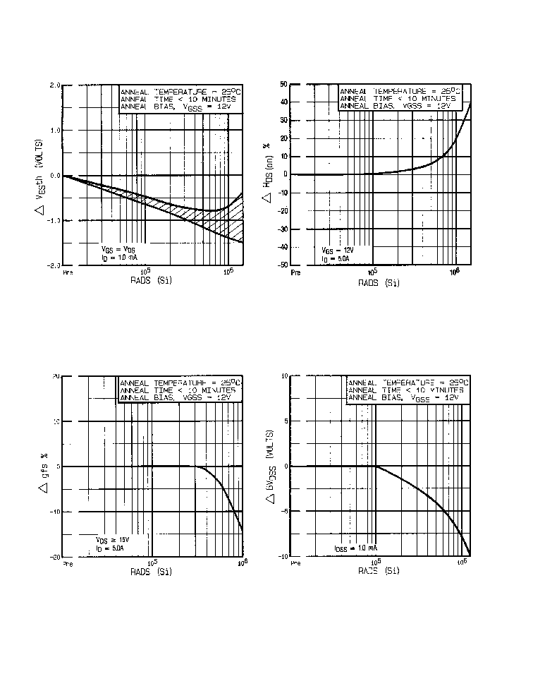
Fig 2. Typical Response of On-State Resistance
Vs. Total Dose Exposure
Fig 1. Typical Response of Gate Threshhold
Voltage Vs. Total Dose Exposure
Fig 3. Typical Response of Transconductance
Vs. Total Dose Exposure
Fig 4. Typical Response of Drain to Source
Breakdown Vs. Total Dose Exposure
Post-Irradiation
IRHF7130, IRHF8130,JANSR-,JANSH-,2N7261 Devices
www.irf.com
5
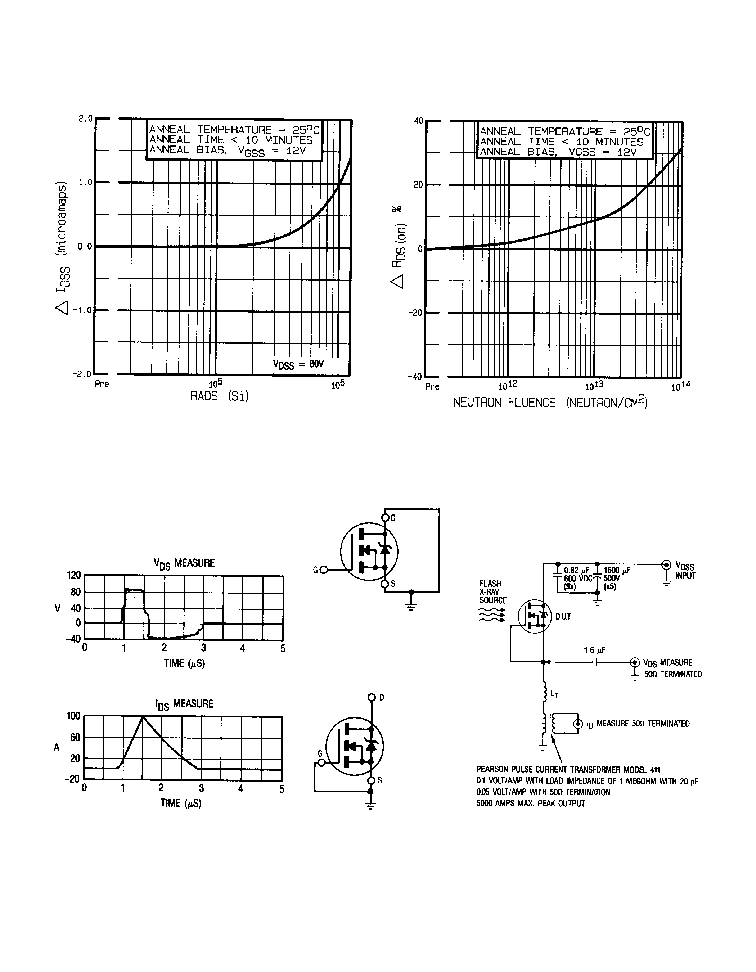
Post-Irradiation
Fig 6. Typical On-State Resistance Vs.
Neutron Fluence Level
Fig 5. Typical Zero Gate Voltage Drain
Current Vs. Total Dose Exposure
Fig 8b. V
DSS
Stress Equals
80% of B
VDSS
During Radiation
Fig 9. High Dose Rate
(Gamma Dot) Test Circuit
Fig 7. Typical Transient Response
of Rad Hard HEXFET During
1x10
12
Rad (Si)/Sec Exposure
IRHF7130, IRHF8130,JANSR-,JANSH-,2N7261 Devices
Fig 8a. Gate Stress of V
GSS
Equals 12 Volts During
Radiation