 | ÐлекÑÑоннÑй компоненÑ: LS2805D | СкаÑаÑÑ:  PDF PDF  ZIP ZIP |
LS-SERIES-28V-S-D.pmd
01/05/06
www.irf.com
1
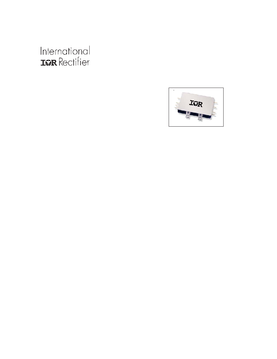
HIGH RELIABILITY LS-SERIES
DC/DC CONVERTER
28V Input, Single/Dual Output
Description
n 18 to 40V DC Input Range
n Total Ionization Dose > 100K Rad(Si)
n SEE LET (Heavy Ions) > 82 MeV·cm
2
/mg
(SEU, SEL, SEGB, SEGR)
n Internal EMI filter; Converter Capable of
meeting MIL-STD-461C CE03
n Low Weight, < 85 grams
n Magnetically Coupled Feedback
n Up to 30W Output Power
n Single and Dual Output Models Include
1.5, 2.5, 3.3, 5, 12, 15,
±5, ±12 and ±15V
n High Efficiency - to 83%
n 100M @ 500VDC Isolation
n Under-Voltage Protection
n Short Circuit and Overload Protection
n Adjustable Output Voltage
n External Inhibit
n > 4,000,000 Hour MTBF (SF)
Features
The LS-Series of DC/DC converters provide same
mechanical outline, power ratings, for backward pin
compatibility, to their lower radiation tolerant counterpart
M3L and Military series ATS DC/DC converters. The
common platform design allows for similarity between
military and space system architectures. For higher
output power applications the HM, M3H and M3G-Series
of DC/DC converters are recommended.
Applications
The LS-Series of DC/DC converters are, high reliability
devices designed for hostile radiation hardened
environments. The LS-Series provide up to 30 watts
output power, small size, low weight, integrated EMI
filtering and a high tolerance to environmental stresses
such as radiation, temperature extremes, mechanical
shock, and vibration. All components are fully de-rated
to meet the requirements of MIL-STD-975. Extensive
documentation including, thermal analysis, stress
analysis and reliability predictions are available.
The LS-Series of converters incorporate a fixed
frequency single forward topology with magnetic
feedback and an internal EMI filter. These converters
are capable of meeting the conducted emissions
requirements of MIL-STD-461C without any additional
components. All models include an external inhibit port
and have an adjustable output voltage. They are
enclosed in a hermetic 1.5" x 2.3" x 0.425" steel package
and weigh less than 85 grams. The package utilizes
rugged ceramic feed-through copper core pins and is
sealed using parallel seam welding.
Non-flight (EM-suffix) versions of the LS-Series
converters are available for system development
purposes. These devices are manufactured with the
same generic active circuit elements but do not
haveguaranteed radiation performance. Variations in
electrical specifications and screening to meet custom
requirements can be accommodated.
All converters are manufactured in a facility certified to
MIL-PRF-38534 Class (K). All processes used to
manufacture the converters have been qualified to
enable various levels of compliant devices. Full
environmental screening includes temperature cycling,
constant acceleration, fine and gross leak, PIND,
radiographics and burn-in.
n Geo Synchronous Satellite
n Low Earth Orbit
n Deep Space Probe
n Communication and Display Systems
n Payload and Experiment LVPS
PD-96964

2
www.irf.com
LS-SERIES
The LS-Series converters utilize a single-ended
forward topology with resonant reset. The nominal
switching frequency is 500kHz. Electrical isolation
and tight output regulation are achieved through the
use of a magnetically coupled feedback. Voltage
feed-forward with duty factor limiting provides high
line rejection and protection against output over
voltage in the event of an internal control loop failure.
Circuit Description
An internal EMI filter allows the converter to meet
the conducted emissions requirements of MIL-STD-
461C on the input power leads.
An external inhibit port is provided to control
converter operation. The converter's operation is
inhibited when this pin is pulled low. It is intended
to be driven by an open collector logic device. The
pin may be left open for normal operation and has a
nominal open circuit voltage of 11V with respect to
the input return (pin 2).
Output current is limited under any load fault
condition to approximately 125% of rated. An
overload condition causes the converter output
voltage to drop below nominal. The converter will
resume normal operation when the load current is
reduced below the current limit point. This protects
the converter from both overload and short circuit
conditions. The current limit point exhibits a slightly
negative temperature coefficient to reduce the
possibility of thermal runaway.
The LS-Series was developed using a proven
conservative design methodology derived from other
space level designs that includes selection of
established reliability components and fully de-
rating to the requirements of MIL-STD-975. A
magnetic feedback circuit is utilized instead of opto
-couplers to minimize temperature, aging and
radiation sensitivity. PSPICE was used extensively
to predict and optimize circuit performance for both
beginning and end-of-life. Thorough design
analyses include stress, thermal, and reliability
(MTBF).
The output voltage of all models can be adjusted
using a single external resistor.
Design Methodology
www.irf.com
3
LS-SERIES
Electrical Performance Characteristics
For Notes to Electrical Performance Characteristics, refer to page 5
1. Input voltage rating is BOL. Input voltage range reduced to
20 to 40VDC for EOL.
2. Meets de-rating per MIL-STD-975
Absolute Maximum Ratings
Input voltage range
- -0.5Vdc to +60Vdc
Output power
- Internally limited
Lead temperature
- +300°C for 10 seconds
Operating temperature - -55°C to +125°C
(Note 13)
Storage temperature
- -55°C to +135°C
Recommended Operating Conditions
Input voltage range
1
- 18Vdc to +40Vdc
Output power
- 0 to Max. Rated
Operating temperature
- -55°C to +85°C
Operating temperature
2
- -55°C to +70°C
Limits
Parameter
Group A
Subgroup
Conditions
-55
°C T
C
+85°C
V
IN
= 28V DC ± 5%, C
L
= 0
unless otherwise specified
Min
Nom
Max
Unit
Input Voltage
18
28
40
V
Output Voltage ( Vout )
LS2801R5S
LS2802R5S
LS2803R3S
LS2805S
LS2812S
LS2815S
LS2805D
LS2812D
LS2815D
LS2801R5S
LS2802R5S
LS2803R3S
LS2805S
LS2812S
LS2815S
LS2805D
LS2812D
LS2815D
1
1
1
1
1
1
1
1
1
2,3
2,3
2,3
2,3
2,3
2,3
2,3
2,3
2,3
I
OUT
= 100% rated load
Note 4
I
OUT
= 100% rated load
Notes 4, 14
1.47
2.47
3.27
4.95
11.88
14.85
±4.95
±11.88
±14.85
1.43
2.43
3.23
4.90
11.76
14.70
±4.90
±11.76
±14.70
1.50
2.50
3.30
5.00
12.00
15.00
±5.00
±12.00
±15.00
1.53
2.53
3.33
5.05
12.12
15.15
±5.05
±12.12
±15.15
1.57
2.57
3.37
5.10
12.24
15.30
±5.10
±12.24
±15.30
V
V
Output power ( P
OUT
)
LS2801R5S
LS2802R5S
LS2803R3S
All Others
1,2,3
V
IN
= 18, 28, 40 Volts, Note 2
0
0
0
0
12
20
25
30
W
Output current ( I
OUT
)
LS2801R5S
LS2802R5S
LS2803R3S
LS2805S
LS2812S
LS2815S
LS2805D
LS2812D
LS2815D
1,2,3
V
IN
= 18, 28, 40 Volts, Note 2
Either Output, Note 3
Either Output, Note 3
Either Output, Note 3
0
0
0
0
0
0
0
0
0
8.0
8.0
7.57
6.0
2.5
2.0
4.8
2.3
1.6
A
Line regulation ( VR
LINE
)
1,2,3
V
IN
= 18, 28, 40 Volts
I
OUT
= 0, 50%, 100% rated, Note 4
-0.5
0.5 %
Load regulation ( VR
LOAD
)
LS2801R5S
LS2802R5S
All others
1,2,3
V
IN
= 18, 28, 40 Volts
I
OUT
= 0, 50%, 100% rated, Note 4
-2.0
-1.2
-1.0
2.0
1.2
1.0
%
Cross regulation ( VR
CROSS
)
LS2805D
LS2812D
LS2815D
1,2,3
V
IN
= 18, 28, 40 Volts
Duals only, Note 5
-5.0
-3.0
-3.0
5.0
3.0
3.0
%
4
www.irf.com
LS-SERIES
Electrical Performance Characteristics
( continued )
For Notes to Electrical Performance Characteristics, refer to page 5
Limits
Parameter
Group A
Subgroup
Conditions
-55
°C T
C
+85°C
V
IN
= 28V DC ± 5%, C
L
= 0
unless otherwise specified
Min
Nom
Max
Unit
Input Current, no load ( I
IN
)
LS2801R5S
LS2802R5S
LS2803R3S
LS2805S
LS2812S
LS2815S
LS2805D
LS2812D
LS2815D
1,2,3
I
OUT
= 0, Pin 4 open
60
60
60
70
70
70
70
100
100
mA
Input current inhibited
1,2,3
Pin 4 shorted to pin 2
8.0
mA
Output Ripple, ( V
RIP
)
LS2801R5S
LS2802R5S
LS2803R3S
LS2805S
LS2812S
LS2815S
LS2805D
LS2812D
LS2815D
1,2,3
V
IN
= 18, 28, 40 Volts
I
OUT
= 100% rated load
Notes 4, 6
35
35
35
50
70
80
80
80
80
mV p-p
Switching frequency ( F
S
)
1,2,3
425
500
575
KHz
Efficiency ( E
FF
)
LS2801R5S
LS2802R5S
LS2803R3S
LS2805S
LS2812S
LS2815S
LS2805D
LS2812D
LS2815D
1,2,3
I
OUT
= 100% rated load
Note 4
61
68
72
78
78
78
79
79
79
64
72
76
82
82
82
83
83
83
%
Enable Input ( Inhibit Function )
open circuit voltage
drive current ( sink )
voltage range
Note 1
9.5
-0.5
12
5.0
50
V
mA
V
Current Limit Point
Expressed as a percentage
of full rated load current
1,2,3 V
out
= 90% of Nominal, Note 4
105
145 %
Power dissipation, load fault (P
D
)
1,2,3
Short Circuit, Overload, Note 8
14 W
Output response to
step load changes (V
TLD
)
4,5,6
Half Load to/from Full Load, Notes 4,9
-300
300 mV
pk
Recovery time,
step load changes (T
TLD
)
4,5,6
Half Load to/from Full Load, Note
4,9,10
200
µs
Output response to
step line changes (V
TLN
)
18V to/from 40V
I
OUT
= 100% rated load, Notes 1,4,11
-300
300 mV
pk
Recovery Time,
step line changes (T
TLN
)
18V to/from 40V
I
OUT
= 100% rated load, Notes
1,4,10,11
200
µs
www.irf.com
5
LS-SERIES
Electrical Performance Characteristics
( continued )
Notes for Electrical Performance Characteristics
Table
1.
Parameter is tested as part of design characterization or after design changes. Thereafter, parameter shall
be guaranteed to the limits specified.
2.
Parameter verified during line and load regulation tests.
3.
Output load current must be distributed such that at least 20% of the total load current is being provided by
one of the outputs.
4.
Load current split equally between outputs on dual output models.
5.
Cross regulation is measured with 20% rated load on output under test while changing the load on the
other output from 20% to 80% of rated.
6.
Guaranteed for a D.C. to 20MHz bandwidth. Tested using a 20KHz to 10MHz bandwidth using the circuit
on page 6.
7.
Capacitive load may be any value from 0 to the maximum limit without compromising dc performance. For
a capacitive load in excess of the maximum limit, consult the factory.
8.
Overload power dissipation is defined as the device power dissipation with the load set such that V
OUT
=
90% of nominal.
9.
Load step transition time
10 µSec.
10. Recovery time is measured from the initiation of the transient to where V
OUT
has returned to within ±1% of
its steady state value.
11. Line step transition time
100 µSec.
12. Turn-on delay time from either a step application of input power or a logic low to a logic high transition on
the inhibit pin (pin 4) to the point where V
OUT
= 90% of nominal.
13. For operation at temperatures between +85°C and 125°C, de-rate the maximum output power linearly from
100% to 75%.
14. End of life (EOL) is
±3%
Limits
Parameter
Group A
Subgroup
Conditions
-55
°C T
C
+85°C
V
IN
= 28V DC ± 5%, C
L
= 0
unless otherwise specified
Min
Nom
Max
Unit
Turn-on Overshoot (V
OS
)
LS2801R5S
LS2802R5S
LS2803R3S
LS2805S
LS2812S
LS2815S
LS2805D
LS2812D
LS2815D
Turn-on Delay (T
DLY
)
4,5,6
10% Load, Full Load
Notes 4,12
0
150
250
330
500
1000
1000
500
1000
1000
10
mV
ms
Capacitive Load (CL)
LS2801R5S
LS2802R5S
LS2803R3S
LS2805S
LS2812S
LS2815S
LS2805D
LS2812D
LS2815D
I
OUT
= 100% rated load
No effect on DC performance
Notes 1, 4, 7
Each output on duals
Nom
Max
35
35
35
50
70
80
80
80
80
µF
Line Rejection
1
I
OUT
= 100% rated load
DC to 50KHz, Notes 1, 4
35 50
dB
Isolation 1
Input to Output or Any Pin to Case
except pin 3, test @ 500VDC
100
M
Device Weight
85 g
MTBF
MIL-HDBK-217F2, SF, 35
°C
4.0 x 10
6
Hours