Äîêóìåíòàöèÿ è îïèñàíèÿ www.docs.chipfind.ru

SCHOTTKY RECTIFIER
40 Amp
MBR4045CT
MBRB4045CT
MBR4045CT-1
Bulletin PD-20051 rev. A 09/01
1
www.irf.com
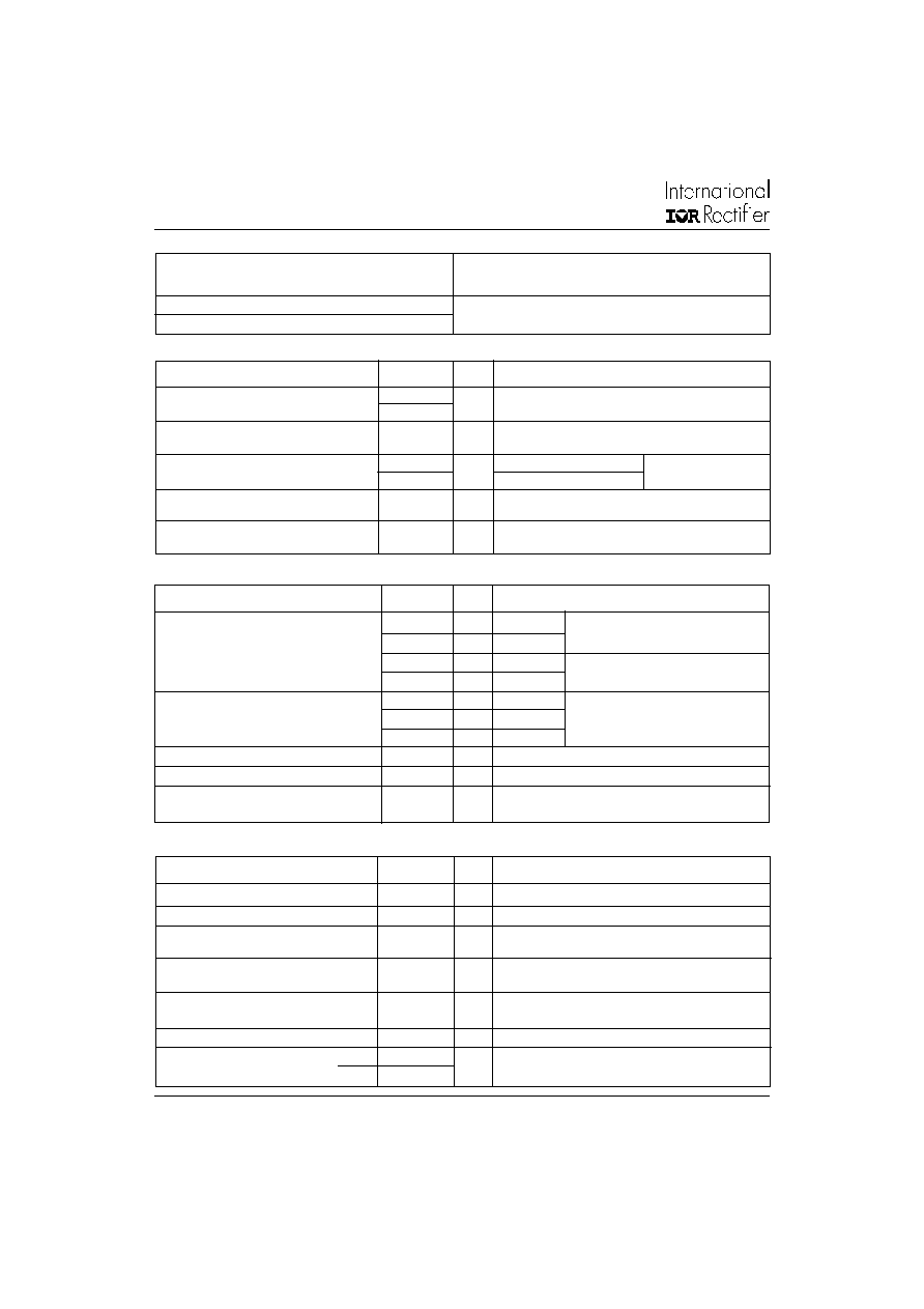
Major Ratings and Characteristics
I
F(AV)
Rectangular waveform
40
A
(Per Device)
I
FRM
@
T
C
= 118°C
40
A
(Per Leg)
V
RRM
45
V
I
FSM
@ tp = 5 µs sine
900
A
V
F
@
20 Apk, T
J
= 125°C
0.58
V
T
J
range
- 65 to 150
°C
Characteristics
Values
Units
Description/Features
This center tap Schottky rectifier has been optimized for low
reverse leakage at high temperature. The proprietary barrier
technology allows for reliable operation up to 150° C junction
temperature. Typical applications are in switching power
supplies, converters, free-wheeling diodes, and reverse bat-
tery protection.
150° C T
J
operation
Center tap TO-220, D
2
Pak and TO-262 packages
Low forward voltage drop
High purity, high temperature epoxy encapsulation for
enhanced mechanical strength and moisture resistance
High frequency operation
Guard ring for enhanced ruggedness and long term
reliability
MBR4045CT
TO-220AB
Case Styles
MBRB4045CT
D
2
PAK
MBR4045CT-1
TO-262
Anode
1
3
2
Base
Common
Cathode
2
Anode
Common
Cathode
Anode
1
3
2
Base
Common
Cathode
2
Anode
Common
Cathode
Anode
1
3
2
Base
Common
Cathode
2
Anode
Common
Cathode
MBR4045CT, MBRB4045CT, MBR4045CT-1
PreBulletin PD-20051 rev. A 09/01
www.irf.com
2
MBR4045CT
MBRB4045CT
MBR4045CT-1
T
J
Max. Junction Temperature Range
-65 to 150
°C
T
stg
Max. Storage Temperature Range
-65 to 175
°C
R
thJC
Max. Thermal Resistance
1.5
°C/W DC operation
Junction to Case (Per Leg)
R
thCS
Typical Thermal Resistance
0.50
°C/W Mounting surface, smooth and greased
Case to Heatsink
Only for TO-220
R
thJA
Max. Thermal Resistance
50
°C/W DC operation
Junction to Ambient
For D
2
Pak and TO-262
wt
Approximate Weight
2 (0.07)
g (oz.)
T
Mounting Torque
Min.
6 (5)
Non-lubricated threads
Max.
12 (10)
Thermal-Mechanical Specifications
Parameters
Values
Units Conditions
Kg-cm
(Ibf-in)
V
FM
Max. Forward Voltage Drop
0.60
V
@ 20A
T
J
= 25 °C
0.78
V
@ 40A
(1)
0.58
V
@ 20A
T
J
= 125 °C
0.75
V
@ 40A
I
RM
Max. Instantaneus Reverse Current
1
mA
T
J
= 25 °C
Rated DC voltage
(1)
50
mA
T
J
= 100 °C
95
mA
T
J
= 125 °C
C
T
Max. Junction Capacitance
900
pF
V
R
= 5V
DC
, (test signal range 100Khz to 1Mhz) 25°C
L
S
Typical Series Inductance
8.0
nH
Measured from top of terminal to mounting plane
dv/dt Max. Voltage Rate of Change
10,000
V/ µs
(Rated V
R
)
Electrical Specifications
Parameters
Values
Units Conditions
(1) Pulse Width < 300µs, Duty Cycle <2%
I
F(AV)
Max. Average Forward (Per Leg)
20
A
@ T
C
= 118° C, (Rated V
R
)
Current
(Per Device)
40
I
FRM
Peak Repetitive Forward
40
A
Rated V
R
, square wave, 20kHz
Current
(Per Leg)
T
C
= 118° C
I
FSM
Max.Peak One Cycle Non -Repetitive
900
A
5µs Sine or 3µs Rect. pulse
Surge Current
(Per Leg)
210
10ms Sine or 6ms Rect. pulse
E
AS
Non -Repetitive Avalanche Energy
20
A
T
J
= 25°C, I
AS
= 3Amps, L = 4.40mH
(Per Leg)
I
AR
Repetitive Avalanche Current
3
A
Current decaying linearty to zero in 1 µsec
(Per Leg)
Frequency limited by T
J
max. V
A
= 1.5 x V
R
typical
Absolute Maximum Ratings
Parameters
Values
Units Conditions
Following any rated load
condition and with rated
V
RRM
applied
V
R
Max. DC Reverse Voltage (V)
V
RWM
Max. Working Peak Reverse Voltage (V)
45
Voltage Ratings
Parameters
MBR4045CT, MBRB4045CT, MBR4045CT-1
Bulletin PD-20051 rev. A 09/01
3
www.irf.com
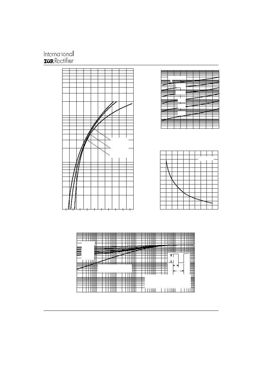
Fig. 2 - Typical Values Of Reverse Current
Vs. Reverse Voltage (Per Leg)
Fig. 3 - Typical Junction Capacitance
Vs. Reverse Voltage (Per Leg)
Fig. 4 - Max. Thermal Impedance Z
thJC
Characteristics (Per Leg)
Fig. 1 - Max. Forward Voltage Drop Characteristics
(Per Leg)
Instantaneous Forward Current - I
F
(A)
Forward Voltage Drop - V
FM
(V)
Reverse Voltage - V
R
(V)
Reverse Current - I
R
(mA)
Reverse Voltage - V
R
(V)
Junction Capacitance - C
T
(p F)
t
1
, Rectangular Pulse Duration (Seconds)
Thermal Impedance Z
thJC
(°C/W)
1
10
100
1000
0
0.2 0.4 0.6 0.8
1
1.2 1.4 1.6 1.8
2
T = 150°C
T = 125°C
T = 25°C
J
J
J
0.001
0.01
0.1
1
10
100
1000
0
5
10 15 20 25 30 35 40 45
125°C
100°C
75°C
50°C
25°C
T = 150°C
J
0.001
0.01
0.1
1
10
0.00001
0.0001
0.001
0.01
0.1
1
10
Single Pulse
(Thermal Resistance)
D = 0.75
D = 0.50
D = 0.33
D = 0.25
D = 0.20
Notes:
1. Duty factor D = t1/ t2
2. Peak Tj = Pdm x ZthJC + Tc
2
t
1
t
P
DM
200
300
400
500
600
700
800
900
0
10
20
30
40
50
T = 25°C
J

MBR4045CT, MBRB4045CT, MBR4045CT-1
PreBulletin PD-20051 rev. A 09/01
www.irf.com
4
Fig. 7 - Max. Non-Repetitive Surge Current (Per Leg)
Fig. 5 - Max. Allowable Case Temperature
Vs. Average Forward Current
Fig. 6 - Forward Power Loss Characteristics
(2) Formula used: T
C
= T
J
- (Pd + Pd
REV
) x R
thJC
;
Pd = Forward Power Loss = I
F(AV)
x V
FM
@ (I
F(AV)
/
D) (see Fig. 6);
Pd
REV
= Inverse Power Loss = V
R1
x I
R
(1 - D); I
R
@ V
R1
= rated V
R
Average Forward Current - I
F(AV)
(A)
Allowable Case Temperature (°C)
Average Forward Current - I
F(AV)
(A)
Average Power Loss (Watts)
Square Wave Pulse Duration - t
p
(microsec)
Non-Repetitive Surge Current - I
FSM
(A)
80
100
120
140
160
0
5
10
15
20
25
30
DC
see note (2)
Square Wave (D = 0.50)
Rated Vr Applied
0
2
4
6
8
10
12
14
16
18
20
0
5
10
15
20
25
30
35
DC
RMS Limit
D = 0.75
D = 0.50
D = 0.33
D = 0.25
D = 0.20
100
1000
10
100
1000
10000
At Any Rated Load Condition
And With Rated Vrrm Applied
Following Surge
MBR4045CT, MBRB4045CT, MBR4045CT-1
Bulletin PD-20051 rev. A 09/01
5
www.irf.com
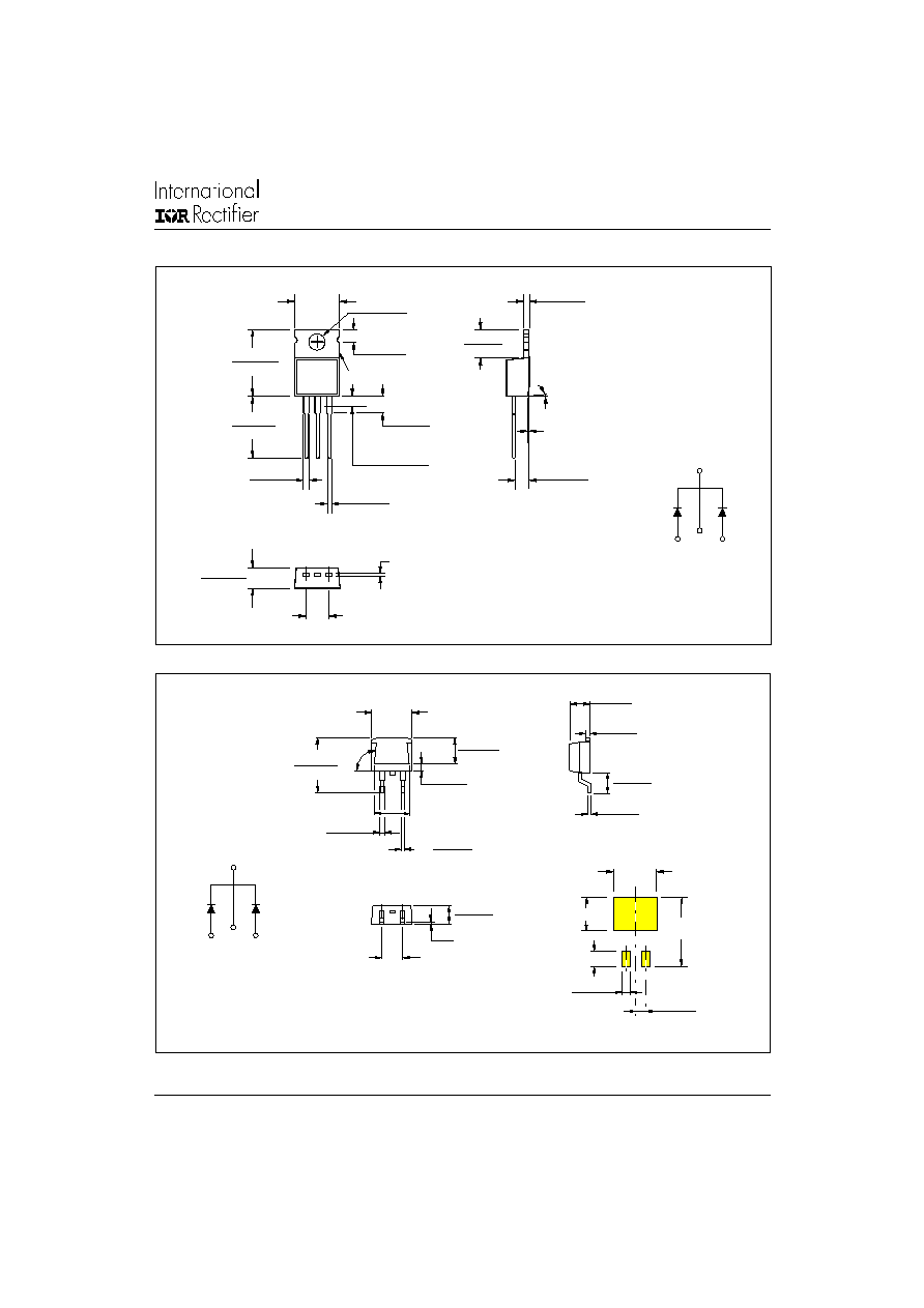
Outline Table
3.78 (0.15)
3.54 (0.14)
10.54 (0.41)
MAX.
DIA.
15.24 (0.60)
14.84 (0.58)
2.92 (0.11)
2.54 (0.10)
1
TERM 2
14.09 (0.55)
13.47 (0.53)
3.96 (0.16)
3.55 (0.14)
0.94 (0.04)
0.69 (0.03)
4.57 (0.18)
4.32 (0.17)
3
0.61 (0.02) MAX.
5.08 (0.20) REF.
1.32 (0.05)
1.22 (0.05)
6.48 (0.25)
6.23 (0.24)
2°
0.10 (0.004)
1.40 (0.05)
1.15 (0.04)
2.89 (0.11)
2.64 (0.10)
1
3
2.04 (0.080) MAX.
2
2
Conform to JEDEC outline TO-220AB
Dimensions in millimeters and (inches)
10.16 (0.40)
REF.
8.89 (0.35)
4.57 (0.18)
4.32 (0.17)
0.61 (0.02) MAX.
5.08 (0.20) REF.
1.32 (0.05)
1.22 (0.05)
1
3
6.47 (0.25)
6.18 (0.24)
93°
REF.
2.61 (0.10)
2.32 (0.09)
5.28 (0.21)
4.78 (0.19)
4.69 (0.18)
4.20 (0.16)
0.55 (0.02)
0.46 (0.02)
14.73 (0.58)
15.49 (0.61)
1.40 (0.055)
1.14 (0.045)
3X
0.93 (0.37)
0.69 (0.27)
2X
11.43 (0.45)
17.78 (0.70)
8.89 (0.35)
3.81 (0.15)
2.08 (0.08)
2X
2.54 (0.10)
2X
MINIMUM RECOMMENDED FOOTPRINT
2
Conform to JEDEC outline D
2
Pak (SMD-220)
Dimensions in millimeters and (inches)
Anode
1
3
2
Base
Common
Cathode
2
Anode
Common
Cathode
Anode
1
3
2
Base
Common
Cathode
2
Anode
Common
Cathode