F E AT U R E S
∑
Rugged, Lightweight Hermetic Ceramic Package
∑
NPT IGBT Technology
∑
Soft Recovery Rectifiers
∑
Zener Gate Protection
∑
Short Circuit Capability
∑
-55 C to +150 C Operating Temperature Range
∑
Hi-Rel Screened Available
DESCRIPTION
C E R M O D TM modules are isolated fully hermetic power modules which combine the latest
NPT IGBT and Soft Recovery Rectifier technology housed in a low thermal resistance
ceramic to metal sealed light weight package. This series of CERMODTM power modules are
offered in a three phase bridge configuration as Phase Leg and chopper configurations.
Designed for tough environments, these high power modules are ideally suited in motor
control, inverters, switching power supplies, in aerospace, defense, transportation and high
power industrial equipment and systems.
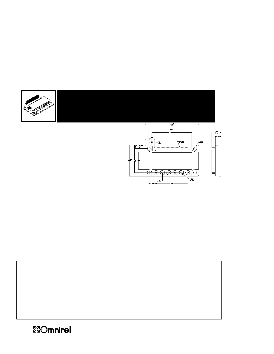
9 5 R0
75 & 100 A, 600V Three Phase Bridge
Configuration in Ceramic to Metal
Sealed Modules
CERMODTM HERMETIC HIGH POWER MODULES,
THREE PHASE BRIDGE, IGBT'S
GENERAL CHARACTERISTICS @ 25
∞
C
OM100L60CMIS, OM75L60CMIS,
OM75L60CMIB
Patent Pending
205 Crawford Street, Leominster, MA 01453 USA (978) 534-5776 FAX (978) 537-4246
Visit Our Web Site at www.omnirel.com
PA R T N U M B E R
VCE, Volts
IC A M P S
VCE (sat) Volts
C O N F I G U R ATION
OM100L60CMIS
600
100
2.5
3 Phase Bridge
OM75L60CMIS
600 75
2.5
3
Phase Bridge
OM75L60CMIB
600
75
2.5
3 Phase Bridge
& Braking Transistor

Rev.05
Omnirel LLC
205 Crawford Street, Leominster, MA 01453
4/15/
99
www.omnirel.com
(978) 534-5776 FAX (978) 537-4246
ELECTRICAL CHARACTERISTICS: (Tc= 25
∞
∞
C unless otherwise specified)
Characteristic
Symbol
Min.
Typ.
Max
Unit
OFF CHARACTERISTICS
Collector Emitter Breakdown Voltage, V
GE
=0V
V
CES
600
V
Zero Gate Voltage Collector Current, V
GE
=0, V
CE
=600V
I
CES
25
µ
A
Gate Emitter Leakage Current, V
GE
=+/-15V, V
CE
=0V
I
GES
2
µ
A
ON CHARACTERISTICS
Gate Threshold Voltage, V
CE
=V
GE,
I
C
=6mA
V
GE(TH)
4.5
6.0
6.5
V
Collector Emitter Saturation Voltage, V
GE
=15V, IC=100A
V
CE(SAT)
2.0
2.5
V
DYNAMIC CHARACTERISTICS
Fwd.
Transconductance
V
CE
=5V, I
C
=100A
gfs
55
S
Input Capacitance
V
GE
=0
Cies
4.5
nF
Output Capacitance
V
CE
=25V
Coes
0.7
nF
Rev. Transfer Capacitance
f=1.0MHz
Cres
1.7
nF
SWITCHING INDUCTIVE LOAD CHARACTERISTICS
Turn-On Delay Time
t(on)
192
nS
Rise Time
V
CC
= 300V, I
C
=100A
tr
81
nS
Turn-on Losses
V
GE
=+15/-10V, R
G
=10
Eon
5.4
mJ
Turn-off Delay Time
L=100
µ
H,Tj=125
∞
C
td(off)
285
nS
Fall Time
tf
44
nS
Turn-off Losses
Eoff
1.4
mJ
DIODE CHARACTERISTICS
Maximum Forward Voltage
I
F
=100A, Tj=25
∞
C
V
F
1.4
1.8
V
Tj=125
∞
C
1.5
1.9
V
R
=300V, Tj=25
∞
C
Qrr
2
µ
C
Reverse Recovery
I
F
=100A, Tj=125
∞
C
3.7
Characteristics
dI/dt=-1080A/
µ
S Tj=25
∞
C
Irr
51
A
Tj=125
∞
C
68
Tj=25
∞
C
trr
124
nS
Tj=125
∞
C
215
THERMAL AND MECHANICAL CHARACTERISTICS
Thermal Resistance, Junction to Case (Per IGBT)R
thJC
0.35
∞
C/W
Thermal Resistance, Junction to Case (Per Diode)
R
thJC
0.6
∞
C/W
Maximum Junction Temperature
T
jMAX
150
∞
C
Isolation Voltage
Vis
RMS
-
V
Screw Torque Mounting
-
15
20
in-
lb
Module Weight
-
250
Grams
OM100L60CMIS
OM100L60CMIS
Rev.05
Omnirel LLC
205 Crawford Street, Leominster, MA 01453 U
4/15/
99
www.omnirel.com
(978) 534-5776 FAX (978) 537-4246
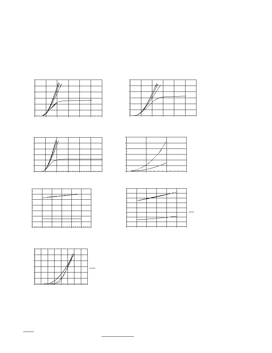
I G B T C o l l e c t o r C u r r e n t v s C o l l e c t o r E m i t t e r
T j = 2 5 C
0
20
40
60
80
100
120
0
1
2
3
4
5
6
V c e ( V )
I c ( A )
9 V g e
1 1 V g e
1 3 V g e
1 5 V g e
I G B T C o l l e c t o r C u r r e n t v s C o l l e c t o r E m i t t e r
T j = + 1 2 5 C
0
20
40
60
80
100
120
0
1
2
3
4
5
6
V c e ( V )
I c ( A )
9 V g e
1 1 V g e
1 3 V g e
1 5 V g e
S w i t c h i n g E n e r g y v s C o l l e c t o r C u r r e n
V c e = 1 0 0 V , T j = 2 5 C
0
1
2
3
4
5
6
0
5 0
1 0 0
1 5 0
Ic(A)
Energy(mJ)
Eon
E o f
S w i t c i n g E n e r g y v s T e m p e r a t u r e V c e = 3 0 0 V , I c =
0
1
2
3
4
5
6
7
0
25
50
75
100
125
150
T ( C )
Energy(mJ)
Eon
E o f
S w i t c h i n g E n e r g y v s G a t e R e s i s t e r
V c e = 3 0 0 V , I c = 1 0 0 , T j = 2 5 C
0
1
2
3
4
5
6
7
8
5
10
15
20
25
30
35
R g ( o h m s )
Energy(mJ)
Eon
Eof
I G B T C o l l e c t o r C u r r e n t v s C o l l e c t o r E m i t t e r
T j = - 5 5 C
0
20
40
60
80
100
120
0
1
2
3
4
5
6
V c e ( V )
I c ( A )
9 V g e
1 1 V g e
1 3 V g e
1 5 V g e
D i o d e F o r w a r d C u r r e n t v s . F o r w a r d V o
V g e = 0 V
0
20
40
60
80
100
120
0
0.25
0.5
0.75
1
1.25
1.5
1.75
2
V f ( V )
I f ( A )
+25C
+125C
-55C
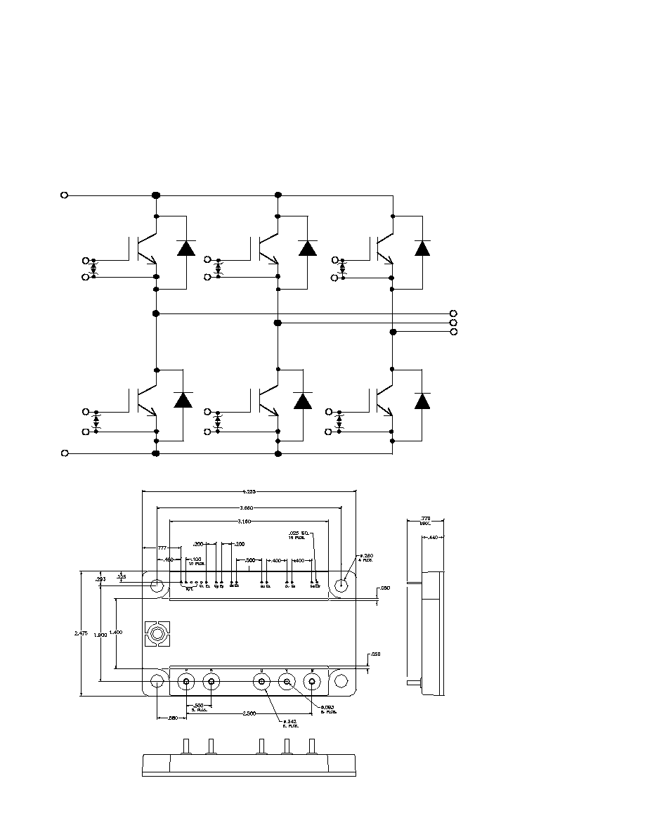
OM100L60CMIS
P
N
U
V
W
Gu
Gv
Ev
Ew
Gx
Ex
Gy
Ey
Gz
Ez
Eu
Gw

OM75L60CMIS
Rev.02
Omnirel LLC 205 Crawford Street,
4/22/99
www.omnirel.com
(978) 534-5776 FAX (978) 537-4246
ELECTRICAL CHARACTERISTICS (Tc= 25
∞
∞
C unless otherwise specified)
Characteristic
Symbol
Min.
Typ.
Max
Unit
OFF CHARACTERISTICS
Collector Emitter Breakdown Voltage, V
CE
=0V
V
CES
600
V
Zero Gate Voltage Collector Current, V
GE
=0, V
CE
=600V
I
CES
25
µ
A
Gate Emitter Leakage Current, V
GE
=+/-15V, V
CE
=0V
I
GES
2
µ
A
ON CHARACTERISTICS
Gate Threshold Voltage, V
CE
=V
GE,
I
C
=6mA
V
GE(TH)
4.5
5.8
6.5
V
Collector Emitter Saturation Voltage, V
GE
=15V, IC=75A
V
CE(SAT)
2.5
2.9
V
DYNAMIC CHARACTERISTICS
Fwd.
Transconductance
V
CE
=5V, I
C
=75A
gfs
36
S
Input Capacitance
V
GE
=0
C
IES
3.7
nF
Output Capacitance
V
CE
=25V
C
OES
1.1
nF
Rev. Transfer Capacitance
f=1.0MHz
C
RES
1.9
nF
SWITCHING INDUCTIVE LOAD CHARACTERISTICS
Turn-On Delay Time
t(on)
60
nS
Rise Time
V
CC
= 300V, I
C
=75A
tr
65
nS
Turn-on Losses
V
GE
=+15/-10V, R
G
=10
Eon
mJ
Turn-off Delay Time
L=100
µ
H,Tj=125
∞
C
td(off)
90
nS
Fall Time
tf
80
nS
Turn-off Losses
Eoff
mJ
DIODE CHARACTERISTICS
Maximum Forward Voltage
I
F
=75A, Tj=25
∞
C
V
F
1.4
2.0
V
Tj=125
∞
C
V
R
=300V, Tj=25
∞
C
Qrr
4
µ
C
Reverse Recovery
I
F
=75A, Tj=125
∞
C
6.5
Characteristics
dI/dt=-1200A/
µ
S Tj=25
∞
C
Irr
40
A
Tj=125
∞
C
Tj=25
∞
C
trr
85
nS
Tj=125
∞
C
THERMAL AND MECHANICAL CHARACTERISTICS
Thermal Resistance, Junction to Case (Per IGBT)R
thJC
0.45
∞
C/W
Thermal Resistance, Junction to Case (Per Diode)
R
thJC
0.8
∞
C/W
Maximum Junction Temperature
T
jMAX
150
∞
C
Isolation Voltage
Vis
RMS
-
V
Screw Torque Mounting
-
15
20
in-
lb
Module Weight
-
250
Grams