 | –≠–ª–µ–∫—Ç—Ä–æ–Ω–Ω—ã–π –∫–æ–º–ø–æ–Ω–µ–Ω—Ç: OM6009SW | –°–∫–∞—á–∞—Ç—å:  PDF PDF  ZIP ZIP |
3.1 - 79
3.1
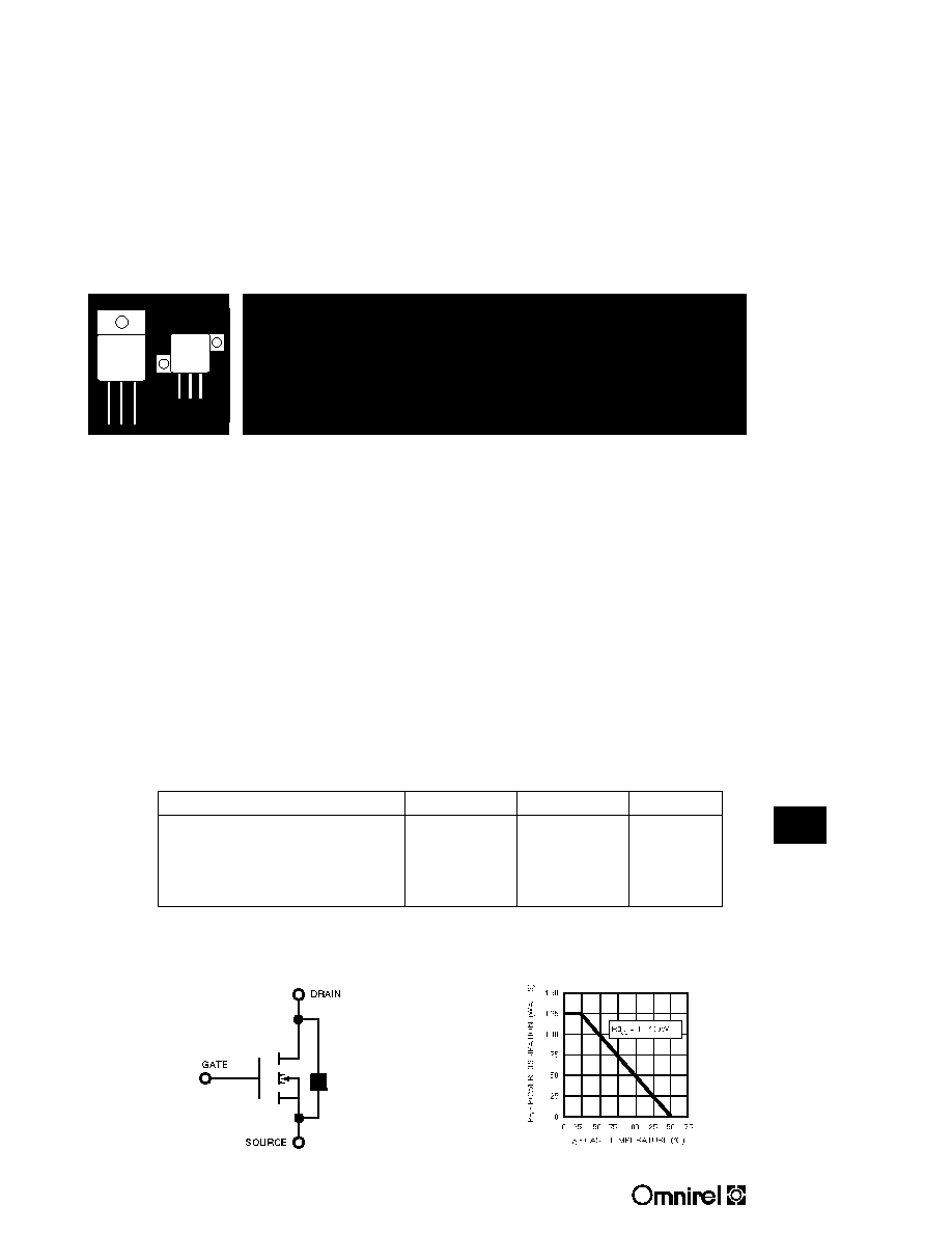
100V Thru 500V, Up To 22 Amp, N-Channel
MOSFET In Hermetic Metal Package, With
Optional Zener Gate Clamp Protection
4 11 R3
Supersedes 1 07 R2
POWER MOSFETS IN HERMETIC ISOLATED
TO-254AA PACKAGE
OM6111SA
OM6112SA
OM6109SA
OM6110SA
OM6011SA
OM6012SA
OM6009SA
OM6010SA
FEATURES
∑ Isolated Hermetic Metal Package
∑ Fast Switching
∑ Low R
DS(on)
∑ Available Hi-Rel Screened To MIL-S-19500, TX, TXV And S Levels
∑ Bi-Lateral Zener Gate Protection (Optional)
∑ Ceramic Feedthroughs Available
DESCRIPTION
This series of hermetically packaged products feature the latest advanced MOSFET
and packaging technology. They are ideally suited for Military requirements where
small size, high performance and high reliability are required, and in applications
such as switching power supplies, motor controls, inverters, choppers, audio
amplifiers and high energy pulse circuits. The MOSFET gates are protected using
bi-lateral zeners in the OM6109SA series.
MAXIMUM RATINGS
PART NUMBER
V
DS
R
DS(ON)
I
D(MAX)
OM6009SA, OM6109SA
100V
.095
22A
OM6010SA, OM6110SA
200V
.18
18A
OM6011SA, OM6111SA
400V
.55
10A
OM6012SA, OM6112SA
500V
.85
8A
SCHEMATIC
POWER RATING
Note: OM61XX Series include gate protection circuitry.
3.1 - 80
OM6009SA - OM6112SA
3.1
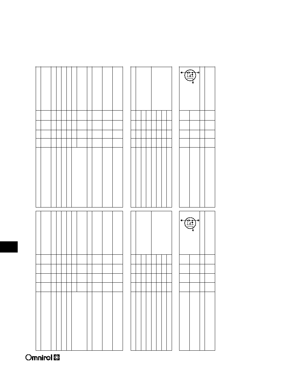
ELECTRICAL CHARACTERISTICS:
T
C
= 25∞ unless otherwise noted
ELECTRICAL CHARACTERISTICS:
T
C
= 25∞ unless otherwise noted
STATIC P/N OM6009SA / OM6109SA
STATIC P/N OM6010SA / OM6110SA
Parameter
Min. Typ. Max. Units Test Conditions
Parameter
Min. Typ. Max. Units Test Conditions
BV
DSS
Drain-Source Breakdown
100
V
V
GS
= 0,
BV
DSS
Drain-Source Breakdown
200
V
V
GS
= 0,
Voltage
I
D
= 250
m
A
Voltage
I
D
= 250
m
A
V
GS(th)
Gate-Threshold Voltage
2.0
4.0
V
V
DS
= V
GS
, I
D
= 250
m
A
V
GS(th)
Gate-Threshold Voltage
2.0
4.0
V
V
DS
= V
GS,
I
D
= 250
m
A
I
GSSF
Gate-Body Leakage Forward
100
nA
V
GS
= 20 V
I
GSSF
Gate-Body Leakage Forward
100
nA
V
GS
= 20 V
I
GSSR
Gate-Body Leakage Reverse
-100
nA
V
GS
= - 20 V
I
GSSR
Gate-Body Leakage Reverse
- 100
nA
V
GS
= - 20 V
I
GSS
Gate-Body Leakage (OM6109)
± 500
nA
V
GS
= ± 12.8 V
I
GSS
Gate-Body Leakage (OM6110)
± 500
nA
V
GS
= ± 12.8 V
I
DSS
Zero Gate Voltage Drain
0.1
0.25
mA
V
DS
= Max. Rat., V
GS
= 0
I
DSS
Zero Gate Voltage Drain
0.1
0.25
mA
V
DS
= Max. Rat., V
GS
= 0
Current
0.2
1.0
mA
V
DS
= 0.8 Max. Rat., V
GS
= 0,
Current
0.2
1.0
mA
V
DS
= 0.8 Max. Rat., V
GS
= 0,
T
C
= 125∞ C
T
C
= 125∞ C
I
D(on)
On-State Drain Current
1
22
A
V
DS
2 V
DS(on)
, V
GS
= 10 V
I
D(on)
On-State Drain Current
1
18
A
V
DS
2 V
DS(on)
, V
GS
= 10 V
V
DS(on)
Static Drain-Source On-State
1.275 1.425
V
V
GS
= 10 V, I
D
= 15 A
V
DS(on)
Static Drain-Source On-State
1.4
1.8
V
V
GS
= 10 V, I
D
= 10 A
Voltage
1
Voltage
1
R
DS(on)
Static Drain-Source On-State
.085 .095
V
GS
= 10 V, I
D
= 15 A
R
DS(on)
Static Drain-Source On-State
0.14
0.18
V
GS
= 10 V, I
D
= 10 A
Resistance
1
Resistance
1
R
DS(on)
Static Drain-Source On-State
.130 .155
V
GS
= 10 V, I
D
= 15 A,
R
DS(on)
Static Drain-Source On-State
0.28
0.36
V
GS
= 10 V, I
D
= 10 A,
Resistance
1
T
C
= 125 C
Resistance
1
T
C
= 125 C
DYNAMIC
DYNAMIC
g
fs
Forward Transductance
1
10.0
S
(
W
)
V
DS
2 V
DS(on)
, I
D
= 15 A
g
fs
Forward Transductance
1
6.0
S
(
W
)
V
DS
2 V
DS(on)
, I
D
= 10 A
C
iss
Input Capacitance
1275
pF
V
GS
= 0
C
iss
Input Capacitance
1000
pF
V
GS
= 0
C
oss
Output Capacitance
550
pF
V
DS
= 25 V
C
oss
Output Capacitance
250
pF
V
DS
= 25 V
C
rss
Reverse Transfer Capacitance
160
pF
f = 1 MHz
C
rss
Reverse Transfer Capacitance
100
pF
f = 1 MHz
T
d(on)
Turn-On Delay Time
16
ns
V
DD
= 30 V, I
D
= 5 A
T
d(on)
Turn-On Delay Time
17
ns
V
DD
= 75 V, I
D
@
18 A
t
r
Rise Time
19
ns
R
g
= 5
W
, V
GS
= 10 V
t
r
Rise Time
52
ns
R
g
= 5
W
, V
GS
= 10 V
T
d(off)
Turn-Off Delay Time
42
ns
T
d(off)
Turn-Off Delay Time
36
ns
t
f
Fall Time
24
ns
t
f
Fall Time
30
ns
BODY-DRAIN DIODE RATINGS AND CHARACTERISTICS
BODY-DRAIN DIODE RATINGS AND CHARACTERISTICS
I
S
Continuous Source Current
- 27
A
Modified MOSPOWER
I
S
Continuous Source Current
- 18
A
Modified MOSPOWER
(Body Diode)
symbol showing
(Body Diode)
symbol showing
I
SM
Source Current
1
- 108
A
the integral P-N
I
SM
Source Current
1
- 72
A
the integral P-N
(Body Diode)
Junction rectifier.
(Body Diode)
Junction rectifier.
V
SD
Diode Forward Voltage
1
- 2.5
V
T
C
= 25 C, I
S
= -24 A, V
GS
= 0
V
SD
Diode Forward Voltage
1
- 2
V
T
C
= 25 C, I
S
= -18 A, V
GS
= 0
t
rr
Reverse Recovery Time
200
ns
T
J
= 150 C,I
F
= I
S
,
t
rr
Reverse Recovery Time
350
ns
T
J
= 150 C,I
F
= I
S
,
dl
F
/ds = 100 A/
m
s
dl
F
/ds = 100 A/
m
s
1 Pulse Test: Pulse Width 300
m
sec, Duty Cycle
2%.
1 Pulse Test: Pulse Width 300
m
sec, Duty Cycle
2%.
(MOSFET) switching times are
essentially independent of
operating temperature.
G
D
S
G
D
S
(MOSFET) switching times are
essentially independent of
operating temperature.
(
W
)
(
W
)
3.1 - 81
OM6009SA - OM6112SA
3.1
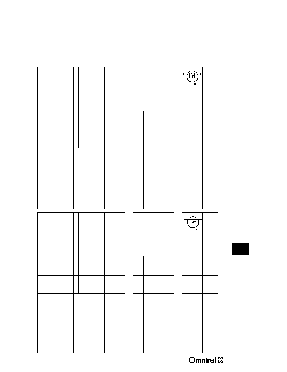
ELECTRICAL CHARACTERISTICS:
T
C
= 25∞ unless otherwise noted
ELECTRICAL CHARACTERISTICS:
T
C
= 25∞ unless otherwise noted
STATIC P/N OM6011SA / OM6111SA
STATIC P/N OM6012SA / OM6112SA
Parameter
Min. Typ. Max. Units Test Conditions
Parameter
Min. Typ. Max. Units Test Conditions
BV
DSS
Drain-Source Breakdown
400
V
V
GS
= 0,
BV
DSS
Drain-Source Breakdown
500
V
V
GS
= 0,
Voltage
I
D
= 250
m
A
Voltage
I
D
= 250
m
A
V
GS(th)
Gate-Threshold Voltage
2.0
4.0
V
V
DS
= V
GS
, I
D
= 250
m
A
V
GS(th)
Gate-Threshold Voltage
2.0
4.0
V
V
DS
= V
GS,
I
D
= 250
m
A
I
GSSF
Gate-Body Leakage Forward
100
nA
V
GS
= 20 V
I
GSSF
Gate-Body Leakage Forward
100
nA
V
GS
= 20 V
I
GSSR
Gate-Body Leakage Reverse
-100
nA
V
GS
= - 20 V
I
GSSR
Gate-Body Leakage Reverse
- 100
nA
V
GS
= - 20 V
I
GSS
Gate-Body Leakage (OM6111)
± 500
nA
V
GS
= ± 12.8 V
I
GSS
Gate-Body Leakage (OM6112)
± 500
nA
V
GS
= ± 12.8 V
I
DSS
Zero Gate Voltage Drain
0.1
0.25
mA
V
DS
= Max. Rat., V
GS
= 0
I
DSS
Zero Gate Voltage Drain
0.1
0.25
mA
V
DS
= Max. Rat., V
GS
= 0
Current
0.2
1.0
mA
V
DS
= 0.8 Max. Rat., V
GS
= 0,
Current
0.2
1.0
mA
V
DS
= 0.8 Max. Rat., V
GS
= 0,
T
C
= 125∞ C
T
C
= 125∞ C
I
D(on)
On-State Drain Current
1
10
A
V
DS
2 V
DS(on)
, V
GS
= 10 V
I
D(on)
On-State Drain Current
1
8.0
A
V
DS
2 V
DS(on)
, V
GS
= 10 V
V
DS(on)
Static Drain-Source On-State
2.35 2.75
V
V
GS
= 10 V, I
D
= 5 A
V
DS(on)
Static Drain-Source On-State
3.2
3.4
V
V
GS
= 10 V, I
D
= 4 A
Voltage
1
Voltage
1
R
DS(on)
Static Drain-Source On-State
0.47 0.55
V
GS
= 10 V, I
D
= 5 A
R
DS(on)
Static Drain-Source On-State
0.8
0.85
V
GS
= 10 V, I
D
= 4 A
Resistance
1
Resistance
1
R
DS(on)
Static Drain-Source On-State
0.93 1.10
V
GS
= 10 V, I
D
= 5 A,
R
DS(on)
Static Drain-Source On-State
1.50
1.65
V
GS
= 10 V, I
D
= 4 A,
Resistance
1
T
C
= 125 C
Resistance
1
T
C
= 125 C
DYNAMIC
DYNAMIC
g
fs
Forward Transductance
1
4.0
S
(
W
)
V
DS
2 V
DS(on)
, I
D
= 5 A
g
fs
Forward Transductance
1
4.0
S
(
W
)
V
DS
2 V
DS(on)
, I
D
= 4 A
C
iss
Input Capacitance
1150
pF
V
GS
= 0
C
iss
Input Capacitance
1275
pF
V
GS
= 0
C
oss
Output Capacitance
165
pF
V
DS
= 25 V
C
oss
Output Capacitance
200
pF
V
DS
= 25 V
C
rss
Reverse Transfer Capacitance
70
pF
f = 1 MHz
C
rss
Reverse Transfer Capacitance
85
pF
f = 1 MHz
T
d(on)
Turn-On Delay Time
17
ns
V
DD
= 175 V, I
D
@
5 A
T
d(on)
Turn-On Delay Time
17
ns
V
DD
= 200 V, I
D
=
4 A
t
r
Rise Time
12
ns
R
g
= 5
W
, V
GS
= 10 V
t
r
Rise Time
5
ns
R
g
= 5
W
, V
GS
= 10 V
T
d(off)
Turn-Off Delay Time
45
ns
T
d(off)
Turn-Off Delay Time
42
ns
t
f
Fall Time
30
ns
t
f
Fall Time
14
ns
BODY-DRAIN DIODE RATINGS AND CHARACTERISTICS
BODY-DRAIN DIODE RATINGS AND CHARACTERISTICS
I
S
Continuous Source Current
- 10
A
Modified MOSPOWER
I
S
Continuous Source Current
- 8
A
Modified MOSPOWER
(Body Diode)
symbol showing
(Body Diode)
symbol showing
I
SM
Source Current
1
- 40
A
the integral P-N
I
SM
Source Current
1
- 32
A
the integral P-N
(Body Diode)
Junction rectifier.
(Body Diode)
Junction rectifier.
V
SD
Diode Forward Voltage
1
- 2
V
T
C
= 25 C, I
S
= -10 A, V
GS
= 0
V
SD
Diode Forward Voltage
1
- 2
V
T
C
= 25 C, I
S
= -18 A, V
GS
= 0
t
rr
Reverse Recovery Time
530
ns
T
J
= 150 C,I
F
= I
S
,
t
rr
Reverse Recovery Time
700
ns
T
J
= 150 C,I
F
= I
S
,
dl
F
/ds = 100 A/
m
s
dl
F
/ds = 100 A/
m
s
1 Pulse Test: Pulse Width 300
m
sec, Duty Cycle
2%.
1 Pulse Test: Pulse Width 300
m
sec, Duty Cycle
2%.
(MOSFET) switching times are
essentially independent of
operating temperature.
(MOSFET) switching times are
essentially independent of
operating temperature.
G
D
S
G
D
S
(
W
)
(
W
)
OM6009SA - OM6112SA
3.1
205 Crawford Street, Leominster, MA 01453 USA (508) 534-5776 FAX (508) 537-4246
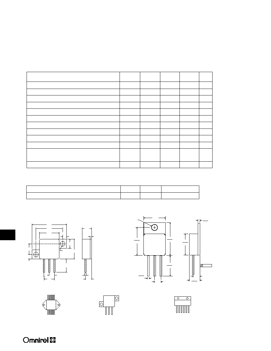
ABSOLUTE MAXIMUM RATINGS (T
C
= 25∞C unless otherwise noted)
OM6009
OM6010
OM6011
OM6012
Parameter
OM6109
OM6110
OM6111
OM6112
Units
V
DS
Drain-Source Voltage
100
200
400
500
V
V
DGR
Drain-Gate Voltage (R
GS
= 1 M )
100
200
400
500
V
I
D
@ T
C
= 25∞C
Continuous Drain Current
2
± 22
± 18
± 10
± 8
A
I
D
@ T
C
= 100∞C
Continuous Drain Current
2
± 17
± 11
± 6
± 5
A
I
DM
Pulsed Drain Current
1
± 88
± 72
± 40
± 32
A
V
GS
Gate-Source Volt. (Unclamped Gate)
± 20
± 20
± 20
± 20
V
P
D
@ T
C
= 25∞C
Maximum Power Dissipation
125
125
125
125
W
P
D
@ T
C
= 100∞C
Maximum Power Dissipation
50
50
50
50
W
Junction To Case
Linear Derating Factor
1.0
1.0
1.0
1.0
W/∞C
Junction To Ambient Linear Derating Factor
.020
.020
.020
.020
W/∞C
T
J
Operating and
T
stg
Storage Temperature Range
-55 to 150
-55 to 150
-55 to 150
-55 to 150
∞C
Lead Temperature
(1/16" from case for 10 secs.)
300
300
300
300
∞C
1 Pulse Test: Pulse width 300 µsec. Duty Cycle 2%.
2 Package Pin Limitation = 25 Amps
THERMAL RESISTANCE
R
thJC
Junction-to-Case
1.0
∞C/W
R
thJA
Junction-to-Ambient
50
∞C/W
Free Air Operation
.144 DIA.
.050
.040
.260
.249
.685
.665
.800
.790
.545
.535
.550
.510
.045
.035
.550
.530
.150 TYP.
.150 TYP.
.005
MECHANICAL OUTLINE
.040 DIA.
3 PLCS.
.150
.260
MAX
.040
.940
.500
MIN.
.150
.125
2 PLCS.
.290
.125 DIA.
2 PLS.
.200
.540
.250
.740
.540
.100
2 PLCS.
.300
1
2
3
1 2 3
Pin 1: Drain
Pin 2: Source
Pin 3: Gate
NOTE:
Standard Products are supplied with glass feedthroughs. For ceramic feedthroughs, add the letter "C" to the part number.
Example - OMXXXXCSA MOSFETs are also available in Z-Tab, dual and quad pak styles - Please call the factory for more information.
PACKAGE OPTIONS
MOD PAK
Z-TAB
6 PIN SIP