3.1 - 65
3.1
50V And 60V Ultra Low R
DS(on)
Power MOSFETs In TO-257 And TO-254
Isolated Packages
4 11 R1
Supersedes 3 02 R0
LOW VOLTAGE, LOW R
DS(on)
POWER MOSFETS
IN HERMETIC ISOLATED PACKAGE
FEATURES
∑ Isolated Hermetic Metal Packages
∑ Ultra Low R
DS(on)
∑ Low Conductive Loss/Low Gate Charge
∑ Available Screened To MIL-S-19500, TX, TXV And S Levels
∑ Ceramic Feedthroughs Available
DESCRIPTION
This series of hermetic packaged MOSFETs are ideally suited for low voltage
applications; battery powered voltage power supplies, motor controls, dc to dc
converters and synchronous rectification. The low conduction loss allows smaller
heat sinking and the low gate charge simpler drive circuitry.
MAXIMUM RATINGS
(Per Device)
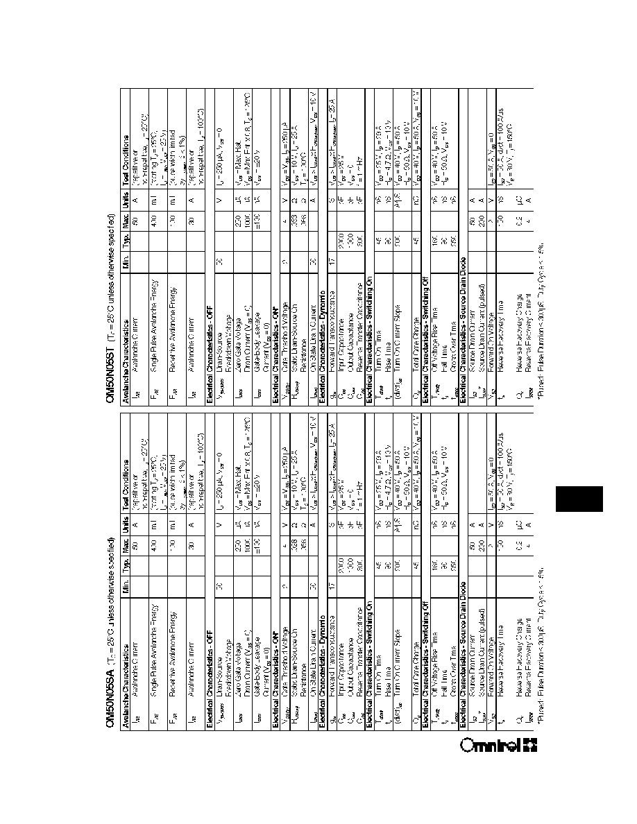
O M 5 0 N 0 6 S T
O M 5 0 N 0 5 S T
O M 6 0 N 0 5 S A
O M 5 0 N 0 5 S A
O M 6 0 N 0 6 S A
O M 5 0 N 0 6 S A
PART NO.
V
DS
(V)
R
DS(on)
( )
I
D
(A)
Package
OM60N06SA
60
.025
60
TO-254AA
OM50N06SA
60
.030
50
TO-254AA
OM50N06ST
60
.035
50
TO-257AA
OM60N05SA
50
.025
60
TO-254AA
OM50N05SA
50
.030
50
TO-254AA
OM50N05ST
50
.035
50
TO-257AA
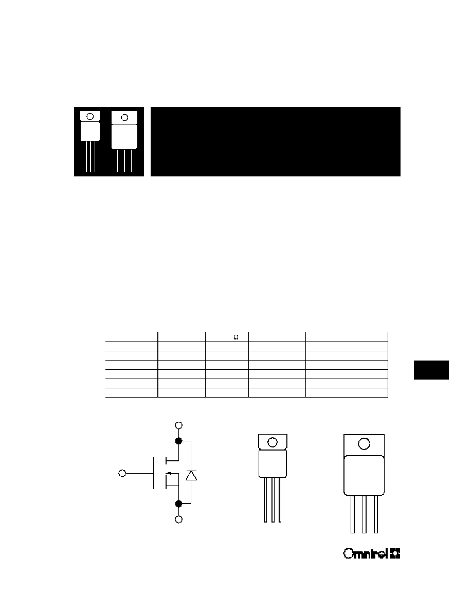
SCHEMATIC
T-3 PIN
CONNECTION
M-PAK PIN
CONNECTION
Drain
Source
Gate
1 2 3
1
2
3
Pin 1: Drain
Pin 2: Source
Pin 3: Gate
Pin 1: Drain
Pin 2: Source
Pin 3: Gate
3.1 - 66
OM60N06SA - OM50N05ST
3.1
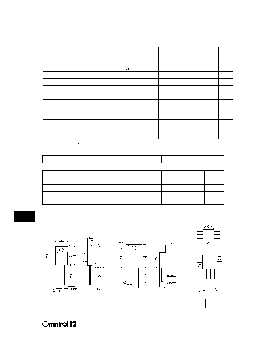
ABSOLUTE MAXIMUM RATINGS (T
C
= 25∞C unless otherwise noted)
50N06ST
50N05ST
Parameter
60N06SA
50N05SA
60N05SA
50N05SA
Units
V
DS
Drain-Source Voltage
60
60
50
50
V
V
DGR
Drain-Gate Voltage (R
GS
= 1 M )
60
60
50
50
V
V
GS
Gate-Source Voltage, Continuous
+20
+20
+20
+20
V
I
D
@ T
C
= 25∞C
Continuous Drain Current
2
55
50
55
50
A
I
D
@ T
C
= 100∞C
Continuous Drain Current
2
37
33
37
33
A
I
DM
Pulsed Drain Current
1
220
200
220
200
A
P
D
@ T
C
= 25∞C
Maximum Power Dissipation
100
100
100
100
W
P
D
@ T
C
= 100∞C
Maximum Power Dissipation
40
40
40
40
W
Junction-To-Case
Linear Derating Factor
1
.80
.80
.80
.80
W/∞C
T
J
Operating and
T
stg
Storage Temperature Range
-55 to 150
-55 to 150
-55 to 150
-55 to 150
∞C
Lead Temperature (1/16" from case for 10 secs.)
300
300
300
300
∞C
1 Pulse Test: Pulse width 300 µsec. Duty Cycle 1.5%.
2 Package Limited SA I
D
= 25 A, SC SC I
D
= 35 A @ 25
∞
C
THERMAL RESISTANCE
R
thJC
Junction-to-Case
1.25
∞C/W
PACKAGE LIMITATIONS
Parameters
TO254AA
TO-257AA
Unit
I
D
Continuous Drain Current
25
15
A
Linear Derating Factor, Junction-to-Ambient
.020
.015
W/∞C
R
thJA
Thermal Resistance, Junction-to-Ambient (Free Air Operation)
50
65
∞C/W
Linear Derating, Junction-to-Case
0.8
0.8
W/∞C
T-3 MECHANICAL OUTLINE
M-PAK MECHANICAL OUTLINE
PACKAGE OPTIONS
MOD PAK
Z-TAB
6 PIN SIP
N o t e s :
∑ Standard Products are supplied with glass feedthroughs. For ceramic feedthroughs, add the letter "C" to the
part number. Example - OMXXXXCSA.
∑ MOSFETs are also available in Z-Pak, dual and quad pak styles. Please call the factory for more information.