 | –≠–ª–µ–∫—Ç—Ä–æ–Ω–Ω—ã–π –∫–æ–º–ø–æ–Ω–µ–Ω—Ç: OM7580SM | –°–∫–∞—á–∞—Ç—å:  PDF PDF  ZIP ZIP |
Ultra Low Dropout, 7.0 A
Adjustable Positive Linear Regulator 5962 - 0323701MXA
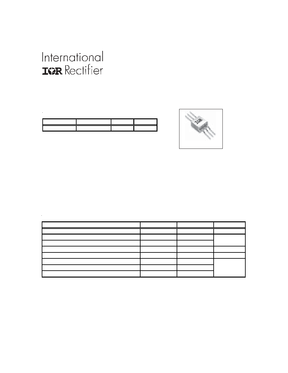
Surface-Mount (SMD-6)
www.irf.com
1
08/06/03
SMD-6
O M 7 5 8 0 S M
Description
Features:
Dropout Voltage of 540mV at Full Load
Dropout Voltage of 100mV at Light Loads
Fast Transient Response
Adjustable Output: 1.8 to 5.5V
Remote Sense
Hermetic SMD-6 Package ensures High
Reliability
The OM7580SM is a 7.0A , ultra low dropout, adjust-
able linear regulator specifically designed for low
voltage, high current applications. Housed in a her-
metic package, the dropout of this device is 540mV
at full load and as low a 100mV at light loads. The
low dropout is achieved by an additional low cur-
rent input voltage. This unit is ideally suited for mili-
tary/defense, commercial aircraft, industrial control
and other harsh environments where a hermetically
sealed package is required.
Absolute Maximum Ratings
Parameter
Symbol
Value
Units
Output Currrent
I
O
7.0
A
Power Input Voltage
V
PWR
6.0
Control Input Voltage
V
CTRL
13
Power Dissipation @ Tc = 25∞C
P
D
20
W
Thermal Resistance, Junction to Case
R
JC
5.0
∞C/W
Operating Junction Temperature Range
T
J
-55 to +125
Storage Temperature Range
T
STG
-65 to +150
∞C
Lead Temperature Soldering (10second maximum)
T
L
300
V
Product Summary
Part Number
Output Voltage
Current
Dropout
OM7580SM
+1.8V to +5.5V
7.0A
0.54V
PD - 94742

2
www.irf.com
OM7580SM
Footnotes
Q
- Denotes specifications which apply over the full operating temperature range.
R
- The minimum load current is minimum current required to maintain regulation. Normally the current in
the resistor divider used to set the output voltage is selected to meet the minimum load current
requirement.
S
- The control pin current is the drive current required for the output transistor. The control pin current is
approximately 0.01% output current. The minimum value is equal to quiescent current of the device.
Electrical Characteristics @T
A
= 25∞C (Unless Otherwise Specified)
Parameter
Test Conditions
Min. Typ. Max. Units
Reference Voltage
V
CTRL
= 2.7V, V
PWR
= 2.0V, I
LOAD
= 10mA
1.243 1.250 1.257
V
ADJ
= 0V
V
CTRL
=2.7 to 12V, V
PWR
=1.75V to 5.5V, I
LOAD
=10mA to 6.0A
Q
1.237 1.250 1.263
Line Regulation
V
CTRL
= 2.5 to 12V, V
PWR
= 3.0V to 5.5V, I
LOAD
= 1.0mA
Q
--
1.0
3.0
Load Regulation
V
CTRL
= 2.75V, V
PWR
= 2.1V, I
LOAD
= 10mA to 6.0A
Q
--
1.0
5.0
Minimum Load Current V
CTRL
= 5.0V, V
PWR
= 3.3V, V
ADJ
= 0V
QR
--
5.0
10
Ground Pin Current
V
CTRL
= 5.0V, V
PWR
= 3.3V, I
LOAD
= 0mA
Q
--
6.0
10
V
CTRL
= 2.75V, V
PWR
= 2.05V, I
LOAD
= 7.0A, TJ = 25∞C
--
--
120
mA
V
CTRL
= 2.75V, V
PWR
= 2.05V, I
LOAD
= 7.0A, TJ = 125∞C
--
--
120
V
CTRL
= 2.75V, V
PWR
= 2.05V, I
LOAD
= 6.0A, TJ = -55∞C
--
--
130
Adjust Pin Current
V
CTRL
= 2.75V, V
PWR
= 2.05V, I
LOAD
= 10mA
--
50
120
µ
A
V
ADJ
= 0V
V
CTRL
= V
PWR
= 5.0V (AVG), V
RIPPLE
= 1.0V
P-P
, f= 120Hz
60
80
--
dB
I
OUT
= 4.0A TJ = 25∞C
V
CTRL
= 2.75V, V
PWR
= 2.05V,
V
OUT
= 100mV, TJ
=
25∞C
7.1
8.0
--
V
CTRL
=2.75V, V
PWR
=2.05V,
V
OUT
=100mV, TJ=-55∞C & TJ=+125∞C
6.6
--
--
V
PWR
= 3.3V, I
LOAD
= 7.0A, TJ = 25∞C
--
--
1.33
V
PWR
= 3.3V, I
LOAD
= 7.0A, TJ = 125∞C
--
--
1.33
V
PWR
= 3.3V, I
LOAD
= 6.0A, TJ = -55∞C
--
--
1.35
V
CTRL
= 2.75V, I
LOAD
= 7.0A, TJ = 25∞C
--
--
0.62
V
CTRL
= 2.75V, I
LOAD
= 7.0A, TJ = 125∞C
--
--
0.80
V
CTRL
= 2.75V, I
LOAD
= 6.0A, TJ = -55∞C
--
--
0.80
Thermal Regulation
V
PWR
= 5.0V, I
O
= 7.0A, P
D
20W, pulse width = 30ms
--
--
0.02
%/W
Dropout is caused by either minimum control voltage or minimum power voltage. Both
Dropout Voltage
parameters are specified with respect to the output voltage. The specifications represent the
minimum input/output voltage required to maintain 1% regulation.
V
V
Minimum V
CONTROL
Minimum V
PWR
V
mV
A
Ripple Rejection
Current Limit
Control Pin Current
S

www.irf.com
3
OM7580SM
Fig 1: Typical Power Voltage Vs Output Current
Fig 2: Typical Control Voltage Vs Output Current
Fig 3: Typical Reference Voltage Vs Temperature
Fig 4: Typical Control Pin Current Vs Output Current
4
www.irf.com
OM7580SM
WORLD HEADQUARTERS: 233 Kansas St., El Segundo, California 90245, Tel: (310) 252-7105
IR LEOMINSTER: 205 Crawford St., Leominster, Massachusetts 01453, Tel: (978) 534-5776
Data and specifications subject to change without notice. 08/03
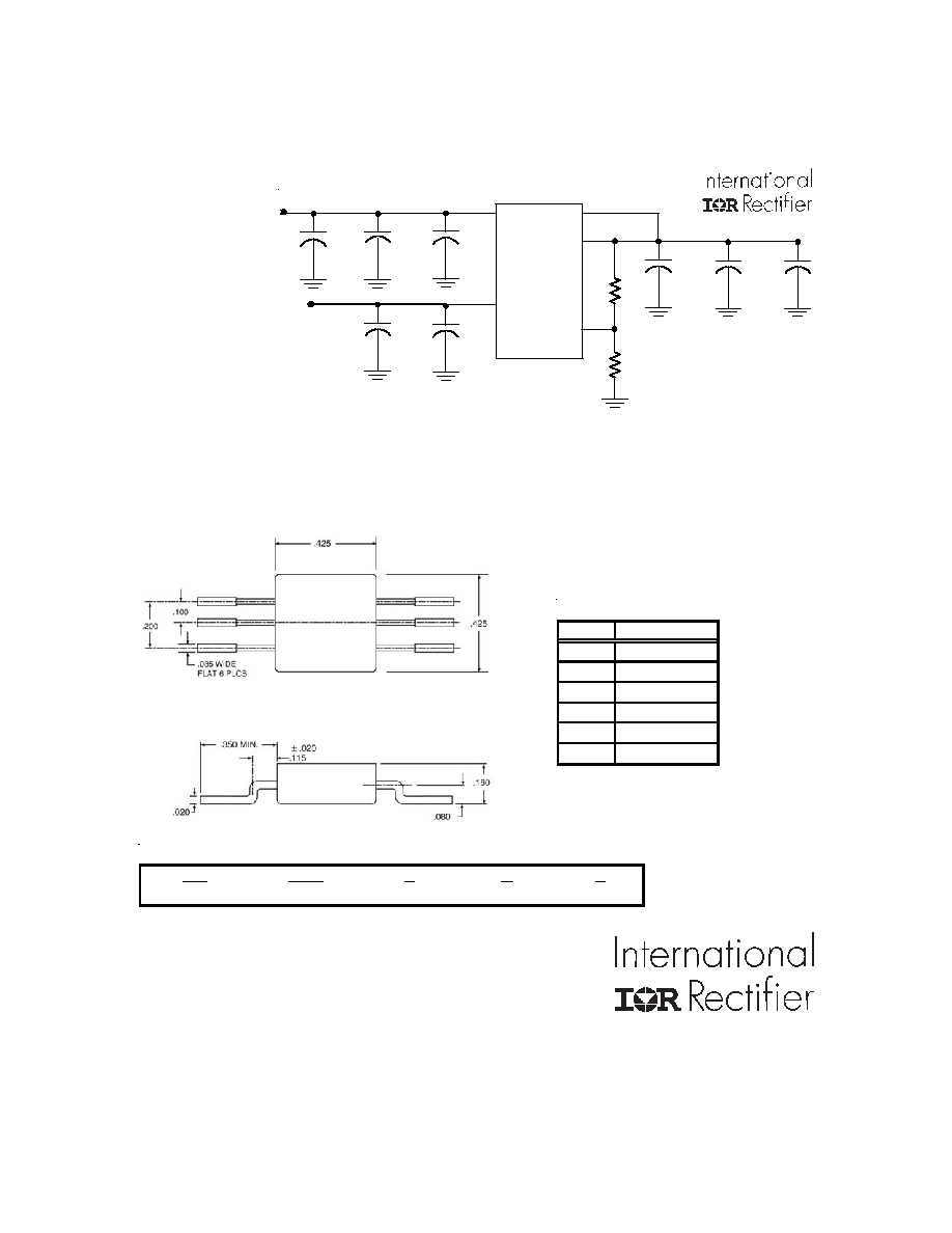
Case Outline and Dimensions
--
SMD-6
Layout Consideration
It is recommended that output capacitors be located as close as possible to the V
OUT
terminal of the
device to prevent any high frequency oscillation that may result due to excessive stray inductance.
Specfications for capacitors: 330
µ
F Tantalum Low ESR, 220
µ
F Electrolytic, 22
µ
F Electrolytic
Pin Assignment
Pin #
Pin Description
1
ADJUST
2
V
OUT
3
V
CTRL
4
V
PWR
5
N/C
6
SENSE
Fig 5: Typical Application
V
OUT
= 1.25V(1 + (R2/R1)) + I
ADJ
(R2)
I
ADJ
= 50uA @ 25∞C
OM7580
V
OUT
Pin1
3.3V
0.1uF
1uF ( x5 )
V
POWER
V
CONTROL
0.1uF
5V
ADJ
R1
R2
Sense
22uF
0.1uF
220uF
1uF ( x5 )
330uF
Pin2
Pin3
Pin4
Pin5
1
2
3
6
4
5
Part Numbering Nomenclature
OM
7580
S
M
X
Omnirel
Device
S=Isolated
Package
Screening