 | –≠–Ľ–Ķ–ļ—ā—Ä–ĺ–Ĺ–Ĺ—č–Ļ –ļ–ĺ–ľ–Ņ–ĺ–Ĺ–Ķ–Ĺ—ā: OMC506 | –°–ļ–į—á–į—ā—Ć:  PDF PDF  ZIP ZIP |
11/24/03
www.irf.com
1
Closed Loop Speed Controller For OMC506
3-Phase Brushless DC Motor
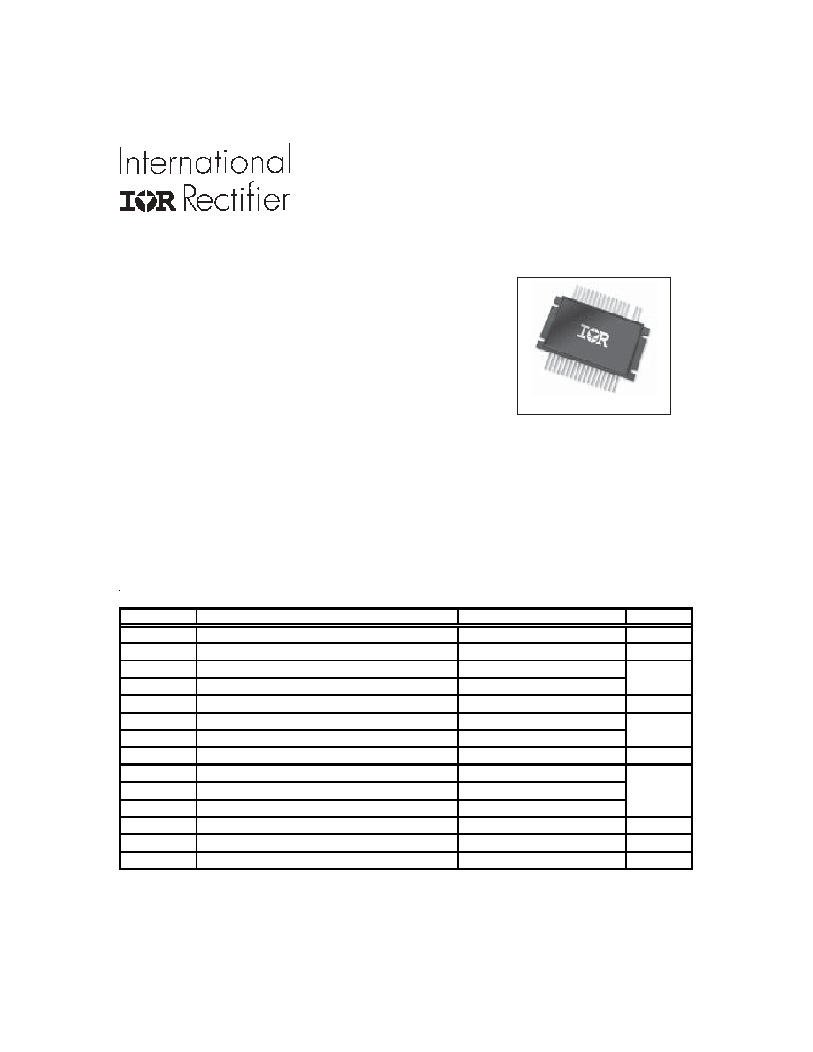
MP-3T Package
Features:
n
10A Average Phase Output Current
n
Over Temperature Protection
n
Compensation Circuitry Adjustable to
Motor Parameters
n
Speed Controlled by 0 to 5V Linear
Input Signal
n
Forward or Reverse Direction
n
Isolated, Low Profile Package
The OMC506 is an integrated, high density, three phase
Brushless DC (BLDC) motor, speed controller housed in a
MP-3Tpackage. The OMC506 contains the power, driver
and control electronics to adjust timing functions and speed
control loop parameters to optimize the controller for each
application. The electronics contained in the OMC506 are
assembled using mixed process technologies: surface
mount components on a printed circuit board and chip &
wire on an Insulated Metal Substrate.This combination
offers small size, excellent thermal characteristics and
electrically isolated heat sink.
MP-3T
Description:
Absolute Maximum Ratings
Symbol
Parameter
Units
V
M
Motor Supply Voltage
Vdc
V
M
pk
Peak Motor Supply Voltage
V
I
O
Average Phase Output Current
I
OP
Pulsed Output Current ( <1% Duty Cycle )
I
OSC
Oscillator Input Current ( Source or Sink )
mA
V
REF
Reference Output Voltage ( I
REF
= 1.0mA )
Digital Inputs ( Fwd / Enable / Brake / SA /SB / SC )
I
REF
Reference Output Current ( V
REF
= 6.2V )
mA
V
SPEED
Speed Control Input Voltage
V
TACH
Tachometer Input Voltage
V
V
CNTL
Temperature Control Input Voltage
Regulator Output Current ( V
REG
+ 15V )
mA
V
CS
Current Sense Input Voltage
V
T
OP
Operating Temperature Range
įC
-25 to 85
-0.3 to 5.0
32
48
10
30
30
-0.3 to V
REF
6.5
V
A
6.2
100
6.5
10
-0.3 to V
REF
PD- 95805

OMC506
2
www.irf.com
A new mixed signal module fully integrates power, control functions, and drive circuitry into a single 2" x 4"
x 0.48" package. The module provides closed loop speed control of three phase, brushless DC (BLDC)
motors used in a variety of system applications. The OMC506 has been designed with flexibility in mind.
Timing functions and loop parameters can be adjusted to optimize the OMC506 to each customer's application.
In addition, the OMC506 has been designed into a MP-3T package. This package uses an insulated metal
substrate, thereby, isolating the module's electronics from chassis while providing the necesssary thermal
interface for proper performance. The OMC506 offers a high efficiency, flexible, compact, motion control
system in an industry standard footprint.
MP3 Package Application
Electrical Characteristics @ T
J
= 25įC (Unless Otherwise Specified)
Characteristics
Parameter
Symbol Min. Typ. Max. Units
Test Conditions
REFERENCE
Reference Output Voltage
V
REF
5.9
6.24
6.5
V
I
REF
= 1.0mA
Reference Load Current
I
REF
-
5.0
8.0
mA
OSCILLATOR
Oscillator Frequency
F
OSC
22
25
28
KHz
Sawtooth Peak Voltage
V
OSCpk
-
4.1
4.5
V
R
OSC
= 4.7K,C
OSC
= 0.01mF
Sawtooth Valley Voltage
V
OSCva
1.2
1.5
-
V
DIGITAL INPUTS
High Input Treshhold Voltage
V
ih
3.0
2.2
-
V
Low Input Treshhold Voltage
V
il
-
1.7
0.8
V
CURRENT SENSE
Treshhold Voltage
V
th
85
101
115
mV
Input Common Mode Volt Range
V
icr
-
3.0
-
V
Input Bias Current
V
ib
-
-0.9
-5.0
mA
VOLTAGE
REGULATOR
Output Voltage
V
reg
14
14.5
15
V
Load Regulation
I
reg
-
0.1
0.3
%
10mA < I
O
< 100mA
THERMAL
Output Trip Voltage
V
OUT
13
13.31 14.79
V
Output Normal Voltage
V
ON
-
0.13
0.4
V
T > T
trip
, R
L
= 100K
Trip Temperature
T
trip
137
145
150
įC
Reset Temperature
T
reset
129
137
142
įC
Internal Current Sense Resistor
R
s
9.5
10
10.5 mOhm
Junction-to-Case MOSFET Resist.
R
thjc
-
-
1.6
įC/W
www.irf.com
3
OMC506
The OMC506 is based on the Motorola MC33035 Brushless Motor Control I.C. This controller is used in
concert with the motorola MC33039 Closed Loop Brushless Motor Adapter I.C. to provide direct duty cycle
control of the motor speed. The OMC506 provides two quadrant speed control via an analog 0 to 5V signal
applied to the Vspeed ( pin22 ) input. The OMC506 is selected for 60/120 degree hall sensor spacing. The
commutation truth table for the OMC506 is shown in Table 1.
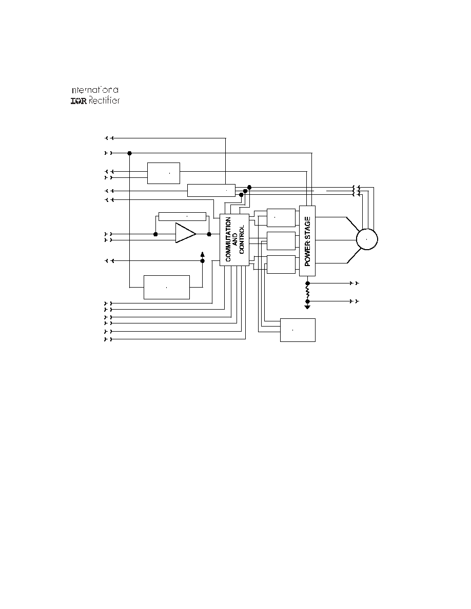
Controller
Block Diagram
RT/CT
V
MOTOR
CONTROL
F
OUT
6.2 V
REF
TACH IN
V
SPEED
+15 V
FWD/REV
OSC
C.S.+
C.S.-
BRAKE
ENABLE
REGULATOR
THREE
PHASE
REFRESH
R
SENSE
R
SENSE
RTN
R
SENSE
C OUT
B OUT
A OUT
MOT
SA
SC
SB
DRIVER
A
DRIVER
B
DRIVER
C
TACHOMETER
COMPENSATION
LOOP
SHAPING
+15 V
V
OUT
OVER
TEMP
CKTRY

OMC506
4
www.irf.com
Additional amplifiers are used in the OMC506 to provide the necessary control loop compensation for extended
bandwidth. By extending the bandwidth of the direct duty cycle control system, torque pertubations can be
accounted for while regulating the speed of the motor. This allows the module to be used in relatively dynamic
systems as well as constant torque applications. Internally, the compensation circuitry used for control loop
shaping can be tuned to optimize the OMC506 for various applications.
The OMC506 provides directional, braking, and enable interfaces from the controller I.C. (pins 32, 24 and 25,
respectively). The module also allows the user to externally set the pulse width modulation (PWW) frequency
(pin21) as well as the pulse width from the Closed Loop Brushless Motor Adapter (pin 34). This allows a
common module to be used in many applications.
Motor commutation and speed control are derived from the Hall effect sensor signals provided from the motor.
The signals are provided as inputs to the OMC506 (pins 29, 30 and 31). The amplitude of the sensor signals
must be limited, by the user, to +6.2V to insure proper operation of the module.
Finally, the output from the Closed Loop Brushless Motor Adapter is provided as an output of the OMC506.
This signal has fixed amplitude and pre-set pulse width. The frequency is six times that of the motor. This
signal is integrated to produce a voltage proportional to motor speed.
Closed Loop Circuit
Table 1 - Commutation Truth Table
SA
SB
SC
F/R
Enable
Brake
A
OUT
B
OUT
C
OUT
Fault
Notes
1
0
0
1
1
0
1
-
0
1
1
1
0
1
1
0
-
1
0
1
0
1
0
1
1
0
0
1
-
1
0
1
1
1
1
0
0
-
1
1
0
0
1
1
1
0
0
-
0
1
1
0
1
1
1
0
1
0
-
1
1
0
0
0
1
0
0
-
1
1
1
1
0
0
1
0
-
0
1
1
0
1
0
0
1
0
1
0
-
1
0
1
1
0
1
0
1
-
0
1
0
0
1
0
1
0
-
1
0
1
1
0
1
0
1
0
0
1
-
1
1
1
1
X
X
0
-
-
-
0
1
0
0
0
X
X
0
-
-
-
0
1
1
1
X
X
1
0
0
0
0
1
0
0
X
X
1
1
0
0
0
0
V
V
V
X
1
1
0
0
0
1
2
V
V
V
X
0
1
0
0
0
0
V
V
V
X
0
0
-
-
-
0
Inputs
Outputs
120
į
Notes:
1) Invalid Sensor Inputs; X= Don't Care
2) V= Valid Sensor Input
www.irf.com
5
OMC506
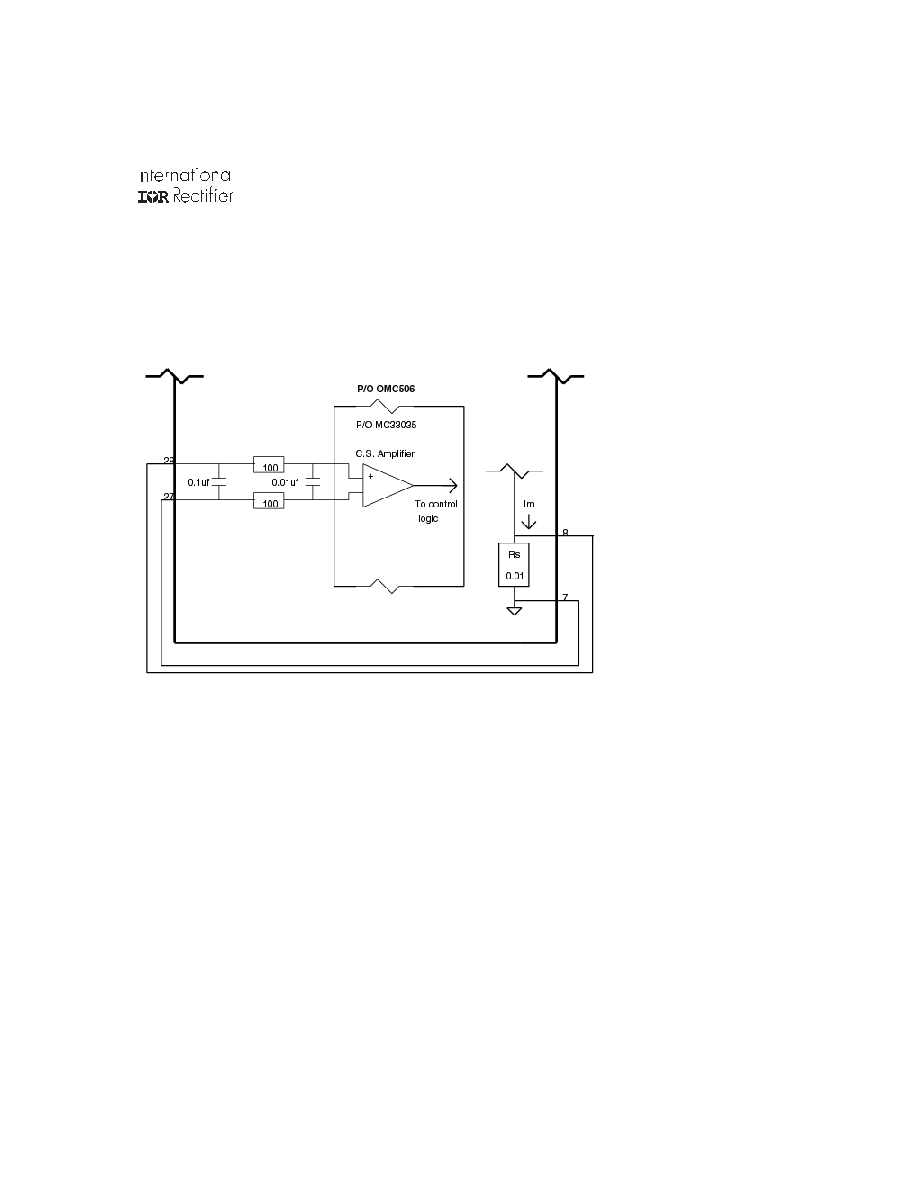
The OMC506 provides outputs from the internal current sense resistor (pin 7& 8). These outputs can be
directly wired to the C.S. +, C.S.- (pin 28 & 27) inputs. The outputs can also be used in external current limit
circuitry. Figure 1 shows a typical connection of the OMC506's current limit circuitry.
Current Limit
Figure 1 - Current Limit Circuitry
The OMC506 has been designed with an internal over temperature protection circuit. The circuit provides a
diagnostic in the event an over temperature condition occurs in the power stage. The circuit normally outputs
a voltage level < 0.5Vdc. When the power stage reaches 140įC, the V
OUT
(pin19) will rise to +15Vdc. The
OMC506 also outputs a control function for this circuitry. A logic "0" at pin 18 will disable the over temperature
circuit and a logic "1" will force V
OUT
to go high. The over temperature circuitry has been designed to interface
with a system controller. The system controller can act on the pretense of an over temperature and shut the
OMC506 down. The system controller may opt to over ride the over temperature flag and disable the circuit
over temperature circuitry. In addition, the system controller can force the V
OUT
high as part of a built in test
(BIT) feature at the system level. The over temperature circuitry will reset when the power stage has cooled to
130įC. Finally, an internal diode can be jumpered causing the temperature circuitry to latch on trip, requiring
a power off reset.
Over Temperature Protection