Äîêóìåíòàöèÿ è îïèñàíèÿ www.docs.chipfind.ru
Applications
!
Telecommunications
!
Load Distribution
!
Industrial Controls
!
Instrumentation and Measurement
!
Electronic Ballast
Data Sheet No. PD10048-F
Series PVI5033R
Photovoltaic Isolator
Solid-State
Opto-Isolated MOSFET Gate Driver
Dual-Channel, 5V, 5
µ
A
General Description
The PVI5033R Photovoltaic Isolator is a dual-
channel, opto-isolated driver capable of directly driving
gates of power MOSFETs or IGBTs. It utilizes a
monolithic integrated circuit photovoltaic generator of
novel construction as its output. The output is controlled
by radiation from a GaAlAs light emitting diode (LED)
which is optically isolated from the photovoltaic
generator.
The PVI5033R is ideally suited for applications
requiring high-current and/or high voltage switching
with optical isolation between the low-level driving
circuitry and high-energy or high- voltage load circuits.
It can be used for directly driving gates of power
MOSFETs. The dual- channel configuration allows its
outputs to drive independent discrete power
MOSFETs, or be connected in parallel or in series to
provide higher-current drive for power MOSFETs or
higher-voltage drive for IGBTs. PVI5033R employs a
fast turn-off circuitry.
PVI5033R Photovoltaic Isolators are packaged in
an 8-pin, molded DIP package with either thru-hole or
"gull-wing" terminals. It is available in standard plastic
shipping tubes or on tape-and-reel. Refer to Part
Identification information.
Part Identification
PVI5033R
thru-hole
PVI5033RS
SMT
PVI5033RS-T SMT, Tape and Reel
Features
!
Monolithic construction
!
3,750 V
RMS
I/O isolation
!
1,200 V
DC
output-to-output isolation
!
Dual-Channel application flexibility
!
Solid-State Reliability
!
UL Recognized and BABT Certified
www.irf.com
1
PVI5033R
2
www.irf.com
GENERAL CHARACTERISTICS
Limits
Units
Min. Dielectric Strength, Input-Output
3750
V
RMS
Min. Dielectric Strength, Output-to-Output
1200
V
DC
Min. Insulation Resistance, Input-to-Output
@TA=+25°C, 50%RH, 100VDC
Max. Capacitance, Input-Output
5.0
pF
Max. Pin Soldering Temperature (10 seconds max.)
+260
°C
Ambient Temperature Range: Operating
-40 to +85
°C
Storage
-40 to +125
°C
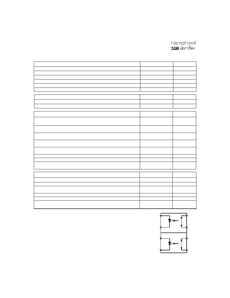
Connection Diagram
10
12
5 (-)
6 (+)
7 (-)
8 (+)
1
2
3
4
COUPLED CHARACTERISTICS
Limits
Units
Min. Output Voltage @ I
LED
= 10mA, R
L
= 10M
5
V
@ T
A
=0°C to +70°C (See Fig. 1 & 2)
Max. Output Voltage @ I
LED
= 10mA, R
L
= 10M
10
V
@ T
A
=0°C to +70°C (See Fig. 1 & 2)
Max. Voltage Differential Between Outputs
1.0
V
@ I
LED
= 5mA, R
L
= 10M
Min. Output Short-Circuit Current
1.65
µA
@ I
LED
= 5mA, @ T
A
=+25°C (See Fig. 1 & 2)
Typical Output Short-Circuit Current
5
µA
@ I
LED
= 10mA, @ T
A
=+25°C (See Fig. 1 & 2)
Max. Turn-On Time @ I
LED
= 5mA, C
LOAD
= 200pF (See Fig. 4)
2.5
ms
Max. Turn-Off Time @ I
LED
= 5mA, C
LOAD
= 200pF (See Fig. 4)
.5
ms
Off-State Clamping Resistance: minimum
350
maximum
1500
OUTPUT CHARACTERISTICS
Limits
Units
Min. Forward Voltage
8.0
V
DC
Max. Reverse Current
10
µA
DC
Electrical Specifications (-40°C
T
A
+85°C unless otherwise specified
)
INPUT CHARACTERISTICS
Limits
Units
Min. Input Current (See Fig.1)
5.0
mA
Input Current Range (See Fig. 1)
3.0 to 25
mA
Max. Continuous Input Current @ T
A
=+25°C
40
mA
LED Forward Voltage Drop @ 5mA, T
A
=+25°C (See Fig. 3)
1.4
V
Max. Reverse Voltage
7.0
V
Max. Reverse Current @ -7V
DC
, T
A
=+25°C
10
µA
International Rectifier does not recommend the use of this
product in aerospace, avionics, military or life support
applications. Users of this International Rectifier product in
such applications assume all risks of such use and in-
demnify International Rectifier against all damages re-
sulting from such use.
PVI5033R
www.irf.com
3
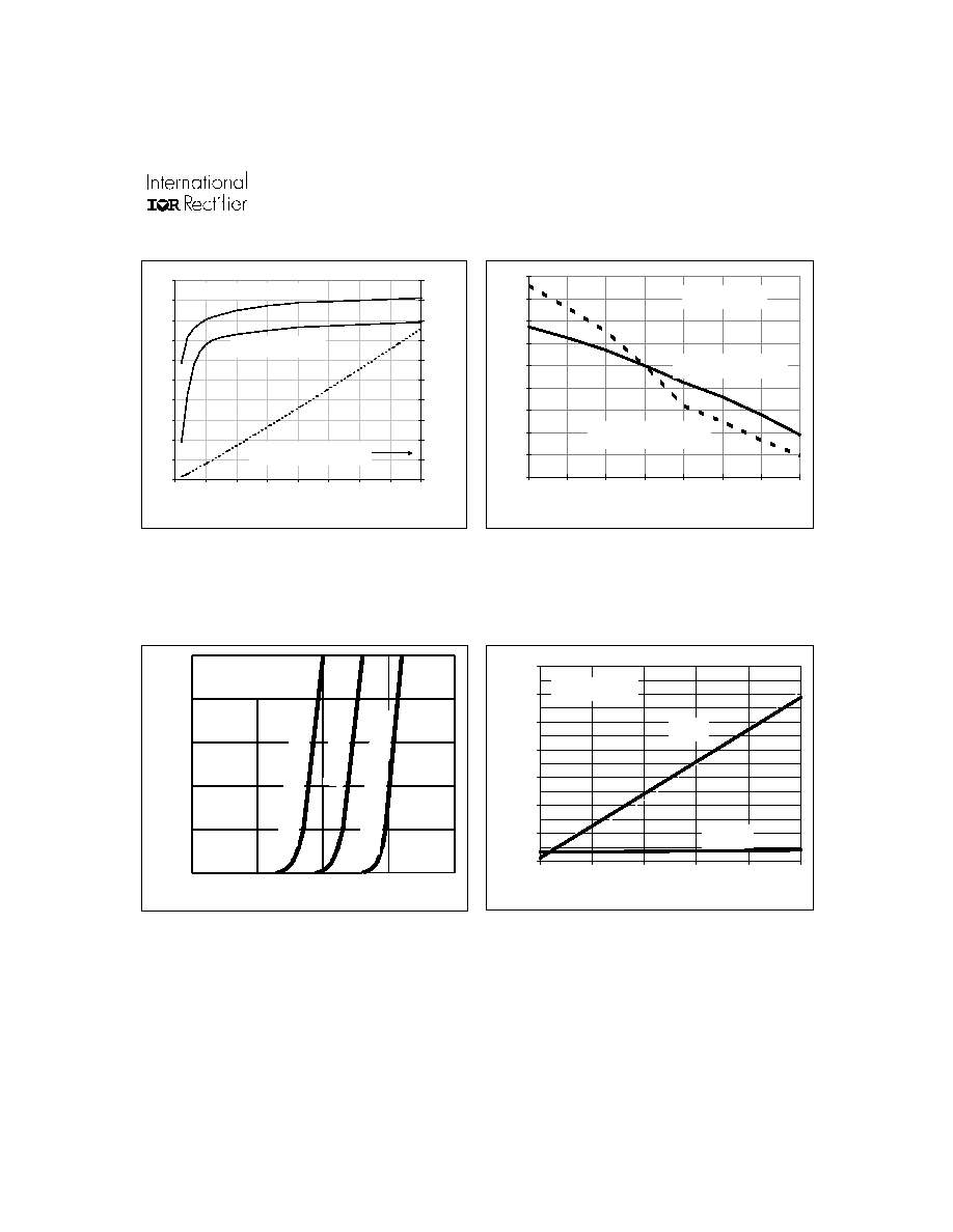
Figure 1. Typical Output Characteristics
Figure 2. Typical Variation of Output
Figure 3. Input Characteristics (Current Controlled)
Figure 4. Typical Response Time
16
20
12
8
4
0
0.5
1.0
1.5
2.0
0
CAUTION: provide current limiting
so that 25 mA maximum steady-
state control current rating is
not exceeded
Input Current (mA)
LED Forward Voltage Drop (Volts DC)
Load Capacitance (pF)
Response T
ime (
µ
s)
Ambient Temperature (deg. C)
Normalized Output
0 200 400 600 800 1000
7000
6000
5000
4000
3000
2000
1000
0
-40 -20 0 25 40 60 85 100
0.5
0.6
0.7
0.8
0.9
1.0
1.1
1.2
1.3
1.4
Short-Circuit Current
Output Voltage
ILED=5mA
ILED=5mA
Ton
Toff
Min. device and +85 deg. C limit
Max. device and -40 deg. C limit
TYPICAL
Input Current (mA)
Output Short-Circuit Current (
µ
A)
0 5 10 15 20 25 30 35 40
30
27
24
21
18
15
12
9
6
3
0
Output V
oltage (V
DC
)
10
9
8
7
6
5
4
3
2
1
0
RL=10M
Open Circuit Voltage
Short Circuit Current
PVI5033R
4
www.irf.com
IR WORLD HEADQUARTERS: 233 Kansas St., El Segundo, California 90245 Tel: (310) 252-7105
Data and specifications subject to change without notice. 10/17/2003
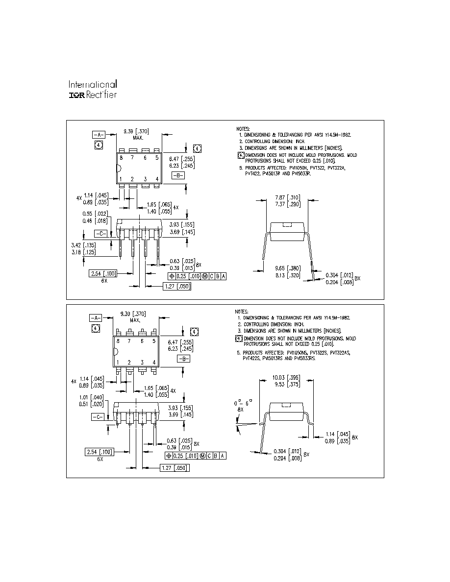
Case Outlines
01-2030 01
01-2031 01