/home/web/doc/html/irf/194479
Data Sheet No. PD 60040E
Series PVT412
Microelectronic Power IC
HEXFET
®
Power MOSFET Photovoltaic Relay
Single Pole, Normally Open,
0-400V, 140mA AC/DC
General Description
The PVT412 Series Photovoltaic Relay is a single-pole,
normally open solid-state relay that can replace
electromechanical relays in many applications. It util-
izes International Rectifier's proprietary HEXFET
power MOSFET as the output switch, driven by an
integrated circuit photovoltaic generator of novel
construction. The output switch is controlled by ra-
diation from a GaAlAs light emitting diode (LED)
which is optically isolated from the photovoltaic gen-
erator.
These SSRs are specifically designed for worldwide
telecom applications. PVT412L employs an active
current-limiting circuitry enabling it to pass FCC Part
68 and other regulatory agency current surge re-
quirements when overvoltage protection is provided.
PVT412 does not employ the current-limiting circuitry
and offers lower on-state resistance.
Series PVT412 Relays are packaged in a 6-lead
molded DIP package with either through-hole or sur-
face mount (`gull-wing') terminals. It is available in
standard plastic shipping tubes or on tape-and-reel.
Please refer to part identification information oppo-
site.
Part Identification
PVT412L
current limit, through-hole
PVT412LS
current limit, surface-mount
PVT412LS-T current limit, surface-mount,
Tape and Reel
PVT412
no current limit, through-hole
PVT412S
no current limit, surface-mount
PVT412S-T
no current limit, surface-mount,
Tape and Reel
Applications
§
On/Off Hook switch
§
Dial-Out relay
§
Ring relay
§
General switching
(HEXFET is the registered trademark for International Rectifier Power MOSFETs)
Features
§
HEXFET Power MOSFET output
§
Bounce-free operation
§
4,000 V
RMS
I/O isolation
§
Load current limiting
§
Linear AC/DC operation
§
Solid-State Reliability
§
UL recognized and BABT certified
§
ESD Tolerance:
4000V Human Body Model
500V Machine Model
Series PVT412
2
www.irf.com
OUTPUT CHARACTERISTICS
PVT412L
PVT412
Operating Voltage Range
0 to ±400
V(DC or AC peak)
Maximum Load Current
@ T
A
=+40°C
5mA Control (see figures1 and 2)
A Connection
120
140
mA (AC or DC)
B Connection
130
150
mA (DC)
C Connection
200
210
mA (DC)
Maximum On-State Resistance
@T
A
=+25°C
For 50mA Pulsed Load, 5mA Control (see figure 4)
A Connection
35
27
B Connection
18
14
C Connection
9
7
Maximum Off-State Leakage
@T
A
=+25°C, ±400V (see figure 5)
1.0
µA
Current Limit
@T
A
=+25°C, For 5mA Control Current:
Connection:
A
C
Minimum
130
260
n/a
mA
Maximum
220
440
n/a
mA
Complies with FCC Part 68 Surge Requirements*
yes
yes
Maximum Turn-On Time
@T
A
=+25°C (see figure 7)
For 50mA, 100 V
DC
load, 5mA Control
2.0
ms
Maximum Turn-Off Time
@T
A
=+25°C (see figure 7)
For 50mA, 100 V
DC
load, 5mA Control
0.5
ms
Maximum Thermal Offset Voltage
@ 5mA Control
0.5
µV
Maximum Output Capacitance
@ 50V
DC
12
pF
GENERAL CHARACTERISTICS
ALL MODELS
Minimum Dielectric Strength, Input-Output
4000
V
RMS
Minimum Insulation Resistance, Input-Output
@T
A
=+25°C, 50%RH, 100V
DC
10
12
Maximum Capacitance, Input-Output
1.0
pF
Maximum Pin Soldering Temperature (10 seconds maximum)
+260
Ambient Temperature Range:
Operating
-40 to +85
°C
Storage
-40 to +100
INPUT CHARACTERISTICS
Part Numbers
Units
PVT412L
PVT412
Minimum Control Current
(see figures 1 and 2)
3.0
mA
Maximum Control Current for Off-State Resistance
0.4
mA
Control Current Range
(Caution: current limit input LED, see figure 6)
3.0 to 25
mA
Maximum Reverse Voltage
7.0
V
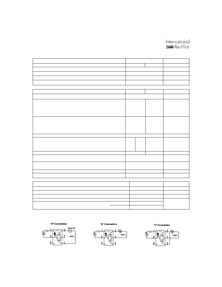
Connection Diagrams
Electrical Specifications (-40°C
T
A
+85°C unless otherwise specified
)
Series PVT412
www.irf.com
3
* Derating of `B' and `C' connection at +85°C will be 70% of that specified at +40°C and is linear from +40°C to +85°C.
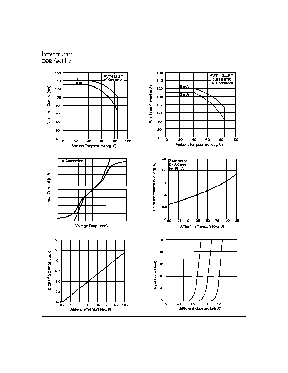
Figure 2. Current Derating Curves*
A
A
ILED=
ILED=
ILED=
I LED=
Figure 1. Current Derating Curves*
Figure 3. Linearity Characteristics
Figure 4. Typical Normalized On-Resistance
PVT412
PVT412L
5 mA control
@ 25°C pulsed
-50
-100
-150
-200
-5.0 -4.0 -3.0 -2.0 -1.0
1.0 2.0 3.0 4.0 5.0
50
100
150
200
Figure 5. Typical Normalized Off-State Leakage
Figure 6. Input Characteristics (Current Controlled)
CAUTION: Provide
current limiting so that
25 mA max. steady-state
control current rating
is not exceeded.
TYPICAL
max.
de
vice & -45
°C limit
min.
d
e
vice & +85
°C limit
Series PVT412
4
www.irf.com
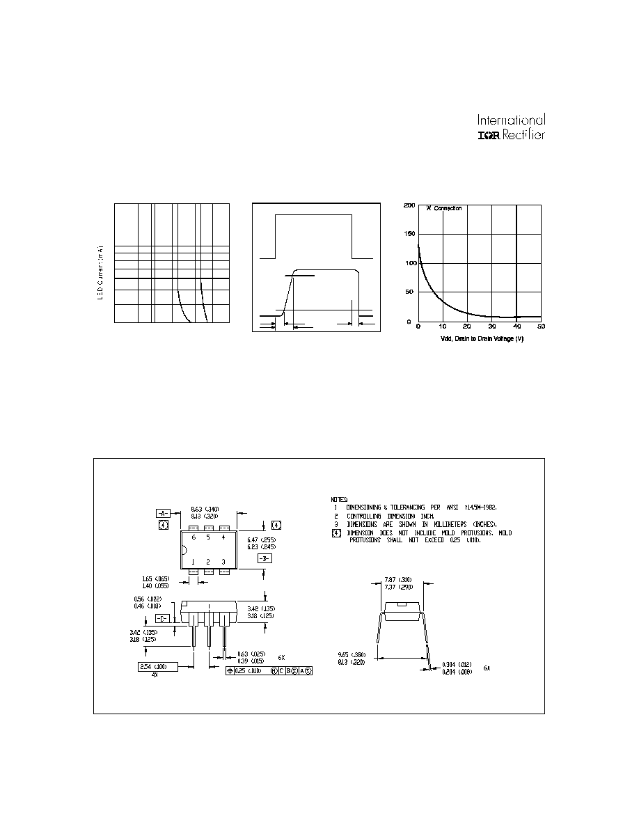
Delay Time (microseconds)
50 100
200
500
20
1000 2000
20
10
5
3
toff
tdly
ton
Figure 7. Typical Delay Times
Figure 9. Typical Output Capacitance
T
ypical Capacitance (pF)
I
D
10%
tdly
ton
toff
ILED
90%
Figure 8. Delay Time Definitions
01-2008 01
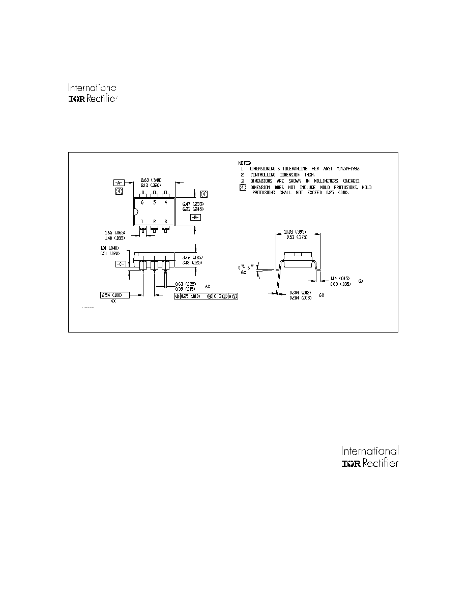
Case Outlines
Series PVT412
www.irf.com
5
IR WORLD HEADQUARTERS: 233 Kansas St., El Segundo, California 90245 Tel: (310) 252-7105
IR EUROPEAN REGIONAL CENTRE: 439/445 Godstone Rd., Whyteleafe, Surrey CR3 0BL, United Kingdom
Tel: ++ 44 (0) 20 8645 8000
IR JAPAN: K&H Bldg., 2F, 30-4 Nishi-Ikebukuro 3-Chome, Toshima-Ku, Tokyo, Japan 171-0021 Tel: 8133 983 0086
IR HONG KONG: Unit 308, #F, New East Ocean Centre, No. 9 Science Museum Road, Tsimshatsui East, Kowloon
Hong Kong Tel: (852) 2803-7380
Data and specifications subject to change without notice. 8/5/2000
01-2009
Case Outlines