RDHA710SE10A2QK.pmd
Radiation Hardended,
Solid-State Relay
with Buffered Inputs
www.irf.com
1
10/26/04
Description
Features:
n
Total Dose Capability to 100krad(Si)
n
Optically Coupled
n
1000V
DC
Input to Output Isolation
n
Buffered Input Stage
n
5.0V Compatible Logic Level Input
n
Controlled Switching Times
n
Hermetically Sealed Package
RDHA710SE10A2QK
Dual 100V, 10A
8-PIN SURFACE MOUNT
For notes, please refer to page 3
The RDHA710SE10A2QK is a radiation hardened
dual solid-state relay in a hermetic package. It is
configured as a dual, single-pole-single-throw
(SPST) normally open relay with common input
supply. This device is characterized for 100 krad(Si)
total ionizing dose. The input and output MOSFETs
utilize International Rectifier's R5 technology. The
RDHA710SE10A2QK is optically coupled and
actuated by standard logic inputs.
Product Summary
g
Part
Breakdown Current
tr / tf
Logic Drive
Number
Voltage
Voltage
RDHA710SE10A2QK
100V
10A
Controlled
5.0V
Absolute Maximum Ratings per Channel @ Tj=25°C (unless otherwise specified)
Parameter
Symbol
Value
Units
Output Supply Voltage
g
V
S
100
V
Output Current
f g
I
O
20
A
Input Buffer Voltage - (pins 4 & 6)
e
V
IN
±10
V
Input Buffer Current
I
IN
±10
mA
Input Supply Voltage (pin 5)
iÃ
V
DD
10
V
Input Supply Current
iÃ
I
DD
25
mA
Power Dissipation
fg
P
DISS
60
W
Operating Temperature Range
T
J
-55 to +125
Storage Temperature Range
T
S
-65 to +150
°C
Lead Temperature
T
L
300
PD - 95876
2
www.irf.com
RDHA710SE10A2QK
For notes, please refer to page 3
Pre-Irradiation
Electrical Characteristics per Channel @ -55°CdT
C
d+125°C
(Unless Otherwise Specified)
Parameter
Group A
Test Conditions
Symbol Min. Typ. Max. Units
Subgroups
1
V
IN
= 5.0V
--
0.070 0.100
2
V
DD
= 5.0V, I
O
= 10A
--
0.115 0.145
Input Buffer Threshold Voltage
ce
V
DD
= 5.0V, I
O
= 10A
V
IN(TH)
4.5
--
--
V
1
V
IN
= 0.8V,
V
S
= 100V
--
--
25
2
V
IN
= 0.8V,
V
S
= 80V
--
--
250
V
DD
= 5.0V, I
O
= 10A
--
10
15
V
DD
= 10V, I
O
= 10A
i
--
--
25
1
--
--
1.0
2,3
--
--
3.0
µA
Input-to-Output Leakage Current
1
V
I-O
= 1.0KVdc, dwell = 5.0s
I
I-O
--
--
1.0
V
IN
=5.0V, V
DD
=5.0V, V
S
=30V
RC = 7.0
/100µF, PW = 50ms
V
IN
=0.8V, V
DD
=5.0V, V
S
=30V
RC = 7.0
/100µF, PW = 50ms
V
IN
=5.0V, V
DD
=5.0V, V
S
=30V
RC = 7.0
/100µF, PW = 50ms
V
IN
=0.8V, V
DD
=5.0V, V
S
=30V
RC = 7.0
/100µF, PW = 50ms
V
IN
= 0.8V, f = 1.0MHz, V
S
=25V
T
C
= 25°C
Thermal Resistance
c
V
IN
= 5.0V, V
DD
= 5.0V
c,f
R
THJC
--
--
1.7
°C/W
MTBF (Per Channel)
MIL-HDBK-217F, SF@Tc= 25°C
6.0
--
--
MHrs
25
t
on
10
t
off
--
t
r
Fall Time
d,h
t
f
1,2,3
pF
365
--
5.5
ms
--
6.5
26
--
6.0
Rise Time
d,h
1,2,3
--
1.3
mA
I
DD
Input Supply Current
c
Output Capacitance
c
C
OSS
--
1,2,3
Turn-On Delay
h
1,2,3
Turn-Off Delay
h
Output On-Resistance
R
DS(ON)
Output Leakage Current
I
O
µA
Input Buffer Current
V
IN
= 5.0V
I
IN
50
www.irf.com
3
RDHA710SE10A2QK
Notes for Maximum Ratings and Electrical Characteristic Tables
Specification is guaranteed by design
Rise and fall times are controlled internally
Inputs protected for V
IN
< 1.0V and V
IN
> 7.5V
m
Optically coupled Solid State Relays (SSRs) have relatively slow turn on and turn off times. Care must be taken to
insure that transient currents do not cause violation of SOA. If transient conditions are present, IR recommends a
complete simulation to be performed by the end user to insure compliance with SOA requirements as specified in the
IRHNJ57130 data sheet
n
While the SSR design meets the design requirements specified in MIL-PRF-38534, the end user is responsible for
product derating, as required for the application
o
Reference Figures 3 & 4 for Switching Test Circuits and Wave Form
Input Supply voltage shall not exceed 5.25V@Tc
70°C
Total Dose Irradiation with Input Bias. 10mA I
DD
applied and V
DS
= 0 during Irradiation
Total Dose Irradiation with Output Bias. 80 Volts V
DS
applied and I
DD
= 0 during Irradiation
Post Total Dose Irradiation
,,
Electrical Characteristics per Channel @ 25°C
(Unless Otherwise Specified)
Parameter
Group A
Test Conditions
Symbol Min. Typ. Max. Units
Subgroups
Output On-Resistance
1
V
IN
= 5.0V, V
DD
= 5.0V, I
O
= 10A
R
DS(ON)
--
0.070 0.100
Output Leakage Current
1
V
IN
= 0.8V,
V
S
= 100V
I
O
--
--
25
Input Buffer Current
1
V
IN
= 5.0V
I
IN
--
--
1.0
V
IN
=5.0V, V
DD
=5.0V, V
S
=30V
RC = 7.0
/100µF, PW = 50ms
V
IN
=0.8V, V
DD
=5.0V, V
S
=30V
RC = 7.0
/100µF, PW = 50ms
V
IN
=5.0V, V
DD
=5.0V, V
S
=30V
RC = 7.0
/100µF, PW = 50ms
V
IN
=0.8V, V
DD
=5.0V, V
S
=30V
RC = 7.0
/100µF, PW = 50ms
t
on
10
t
off
--
t
r
Fall Time
dh
t
f
--
6.0
1
µA
1
Turn-On Delay
h
1
Turn-Off Delay
h
ms
--
6.5
26
25
50
Rise Time
dh
1
--
1.3
5.5
International Rectifier does not currently have a DSCC certified Radiation Hardness Assurance Program
4
www.irf.com
RDHA710SE10A2QK
Radiation Performance
International Rectifier Radiation Hardened MOSFETs are tested to verify their hardness capability. The
hardness assurance program at IR uses a Cobalt-60 (
60
Co) Source and heavy ion irradiation. Both pre- and
post- irradiation performance are tested and specified using the same drive circuitry and test conditions to
provide a direct comparision.
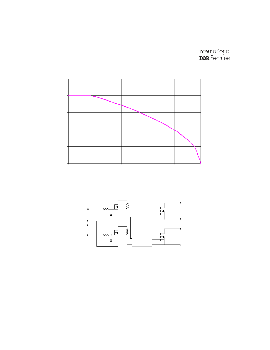
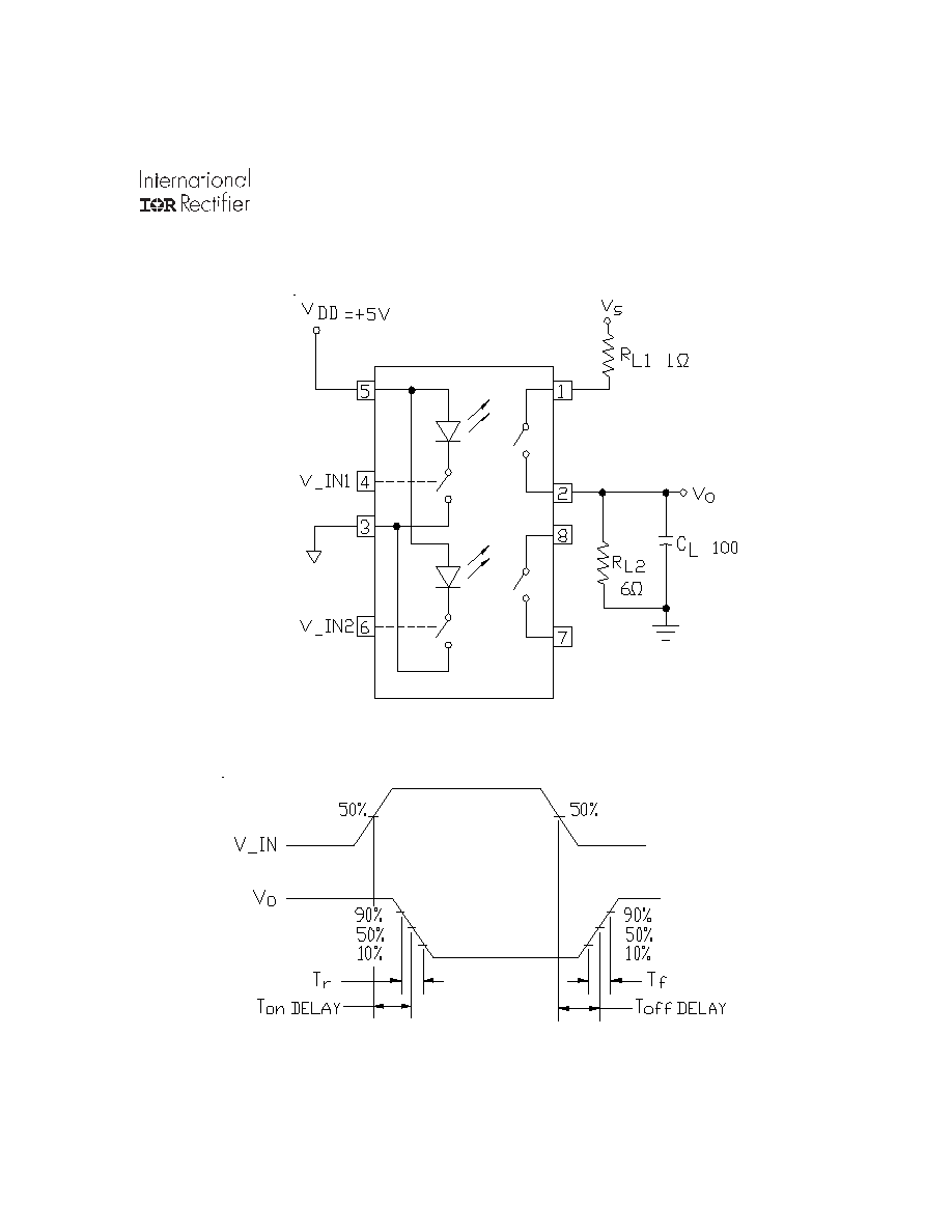
O pto
Isolation
O pto
Isolation
Pin 4 - INPUT 1
Pin 3 - GND
Pin 5 - V
DD
Pin 6 - INPUT 2
Pin 1 - OUT 1+
Pin 2 - OUT 1-
Pin 8 - OUT 2+
Pin 7 - OUT 2-
Fig 2: Typical Application
Fig 1: Maximum Drain Current Vs Case Temperature
0
5
10
15
20
25
25
50
75
100
125
150
T
C
, Case Temperature (°C)
I
D
, Drain Current (A)
www.irf.com
5
RDHA710SE10A2QK
uF
Fig 4: Switching Test Waveform
Fig 3: Switching Test Circuit (Only one channel shown)