 | ÐлекÑÑоннÑй компоненÑ: RF6638 | СкаÑаÑÑ:  PDF PDF  ZIP ZIP |
Control Fet
www.irf.com
1
07/13/06
IRF6638PbF
IRF6638TRPbF
DirectFET
Power MOSFET
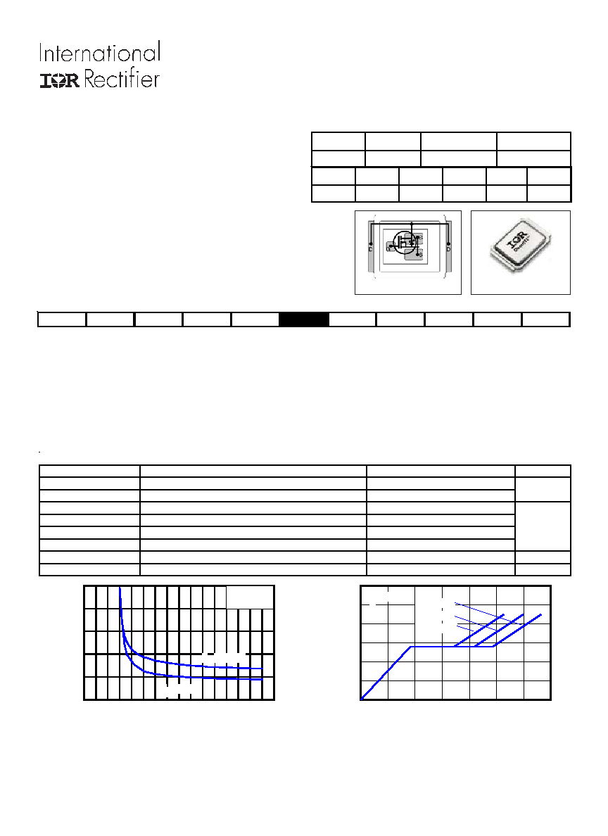
Applicable DirectFET Outline and Substrate Outline (see p.7,8 for details)
Fig 1. Typical On-Resistance Vs. Gate Voltage
Typical values (unless otherwise specified)
Fig 2. Typical Total Gate Charge vs Gate-to-Source Voltage
Click on this section to link to the appropriate technical paper.
Click on this section to link to the DirectFET Website.
Surface mounted on 1 in. square Cu board, steady state.
T
C
measured with thermocouple mounted to top (Drain) of part.
Repetitive rating; pulse width limited by max. junction temperature.
Starting T
J
= 25°C, L = 0.19mH, R
G
= 25
, I
AS
= 20A.
Notes:
DirectFET
ISOMETRIC
PD - 97239
Description
The IRF6638PbF combines the latest HEXFET® Power MOSFET Silicon technology with the advanced DirectFET
TM
packaging to achieve
the lowest on-state resistance in a package that has the footprint of a SO-8 and only 0.6 mm profile. The DirectFET package is compatible
with existing layout geometries used in power applications, PCB assembly equipment and vapor phase, infra-red or convection soldering
techniques, when application note AN-1035 is followed regarding the manufacturing methods and processes. The DirectFET package allows
dual sided cooling to maximize thermal transfer in power systems, improving previous best thermal resistance by 80%.
The IRF6638PbF balances both low resistance and low charge along with ultra low package inductance to reduce both conduction and
switching losses. The reduced total losses make this product ideal for high efficiency DC-DC converters that power the latest generation of
processors operating at higher frequencies. The IRF6638PbF has been optimized for parameters that are critical in synchronous buck
including Rds(on), gate charge and Cdv/dt-induced turn on immunity. The IRF6638PbF offers particularly low Rds(on) and high Cdv/dt
immunity for synchronous FET applications.
MX
SQ
SX
ST
MQ
MX
MT
MP
Absolute Maximum Ratings
Parameter
Units
V
DS
Drain-to-Source Voltage
V
V
GS
Gate-to-Source Voltage
I
D
@ T
A
= 25°C
Continuous Drain Current, V
GS
@ 10V
e
I
D
@ T
A
= 70°C
Continuous Drain Current, V
GS
@ 10V
e
A
I
D
@ T
C
= 25°C
Continuous Drain Current, V
GS
@ 10V
f
I
DM
Pulsed Drain Current
g
E
AS
Single Pulse Avalanche Energy
h
mJ
I
AR
Avalanche Current
Ãg
A
20
Max.
20
140
200
±20
30
25
37
V
DSS
V
GS
R
DS(on)
R
DS(on)
30V max ±20V max 2.2m
@ 10V 3.0m@ 4.5V
0 1 2 3 4 5 6 7 8 9 10 11 12 13 14 15 16
VGS, Gate -to -Source Voltage (V)
0
2
4
6
8
10
T
y
p
i
c
a
l
R
D
S
(
o
n
)
(
m
)
ID = 25A
TJ = 25°C
TJ = 125°C
Q
g tot
Q
gd
Q
gs2
Q
rr
Q
oss
V
gs(th)
30nC
11nC
3.2nC
27nC
18.4nC
1.8V
0
5
10
15
20
25
30
35
QG Total Gate Charge (nC)
0.0
1.0
2.0
3.0
4.0
5.0
6.0
V
G
S
,
G
a
t
e
-
t
o
-
S
o
u
r
c
e
V
o
l
t
a
g
e
(
V
)
VDS= 24V
VDS= 15V
VDS= 6.0V
ID= 20A
l
RoHs Compliant
l
Lead-Free (Qualified up to 260°C Reflow)
l
Application Specific MOSFETs
l
Ideal for CPU Core DC-DC Converters
l
Low Conduction Losses
l
High Cdv/dt Immunity
l
Low Profile (<0.7mm)
l
Dual Sided Cooling Compatible
l
Compatible with existing Surface Mount Techniques
IRF6638PbF
2
www.irf.com
Repetitive rating; pulse width limited by max. junction temperature.
Pulse width
400µs; duty cycle 2%.
Notes:
Static @ T
J
= 25°C (unless otherwise specified)
Parameter
Min. Typ. Max. Units
BV
DSS
Drain-to-Source Breakdown Voltage
30
V
V
DSS
/
T
J
Breakdown Voltage Temp. Coefficient
22
mV/°C
R
DS(on)
Static Drain-to-Source On-Resistance
2.2
2.9
m
3.0
3.9
V
GS(th)
Gate Threshold Voltage
1.35
1.8
2.35
V
V
GS(th)
/
T
J
Gate Threshold Voltage Coefficient
-5.6
mV/°C
I
DSS
Drain-to-Source Leakage Current
1.0
µA
150
I
GSS
Gate-to-Source Forward Leakage
100
nA
Gate-to-Source Reverse Leakage
-100
gfs
Forward Transconductance
105
S
Q
g
Total Gate Charge
30
45
Q
gs1
Pre-Vth Gate-to-Source Charge
6.7
Q
gs2
Post-Vth Gate-to-Source Charge
3.2
nC
Q
gd
Gate-to-Drain Charge
11
Q
godr
Gate Charge Overdrive
9.1
See Fig. 15
Q
sw
Switch Charge (Q
gs2
+ Q
gd
)
14.2
Q
oss
Output Charge
18.4
nC
R
G
Gate Resistance
1.3
t
d(on)
Turn-On Delay Time
19
t
r
Rise Time
45
t
d(off)
Turn-Off Delay Time
28
ns
t
f
Fall Time
6.2
C
iss
Input Capacitance
3770
C
oss
Output Capacitance
810
pF
C
rss
Reverse Transfer Capacitance
410
Diode Characteristics
Parameter
Min. Typ. Max. Units
I
S
Continuous Source Current
3.5
(Body Diode)
A
I
SM
Pulsed Source Current
200
(Body Diode)
g
V
SD
Diode Forward Voltage
1.0
V
t
rr
Reverse Recovery Time
19
29
ns
Q
rr
Reverse Recovery Charge
27
41
nC
di/dt = 300A/µs
i See Fig. 18
T
J
= 25°C, I
S
= 20A, V
GS
= 0V
i
showing the
integral reverse
p-n junction diode.
V
GS
= 4.5V, I
D
= 20A
i
V
DS
= V
GS
, I
D
= 100µA
T
J
= 25°C, I
F
= 20A
V
GS
= 4.5V
I
D
= 20A
V
GS
= 0V
V
DS
= 15V
I
D
= 20A
V
DD
= 16V, V
GS
= 4.5V
c
Conditions
V
GS
= 0V, I
D
= 250µA
Reference to 25°C, I
D
= 1mA
V
GS
= 10V, I
D
= 25A
i
V
GS
= 20V
V
GS
= -20V
V
DS
= 24V, V
GS
= 0V
V
DS
= 15V
V
DS
= 24V, V
GS
= 0V, T
J
= 125°C
MOSFET symbol
Clamped Inductive Load
V
DS
= 15V, I
D
= 20A
Conditions
See Fig. 16 & 17
= 1.0MHz
V
DS
= 16V, V
GS
= 0V
IRF6638PbF
www.irf.com
3
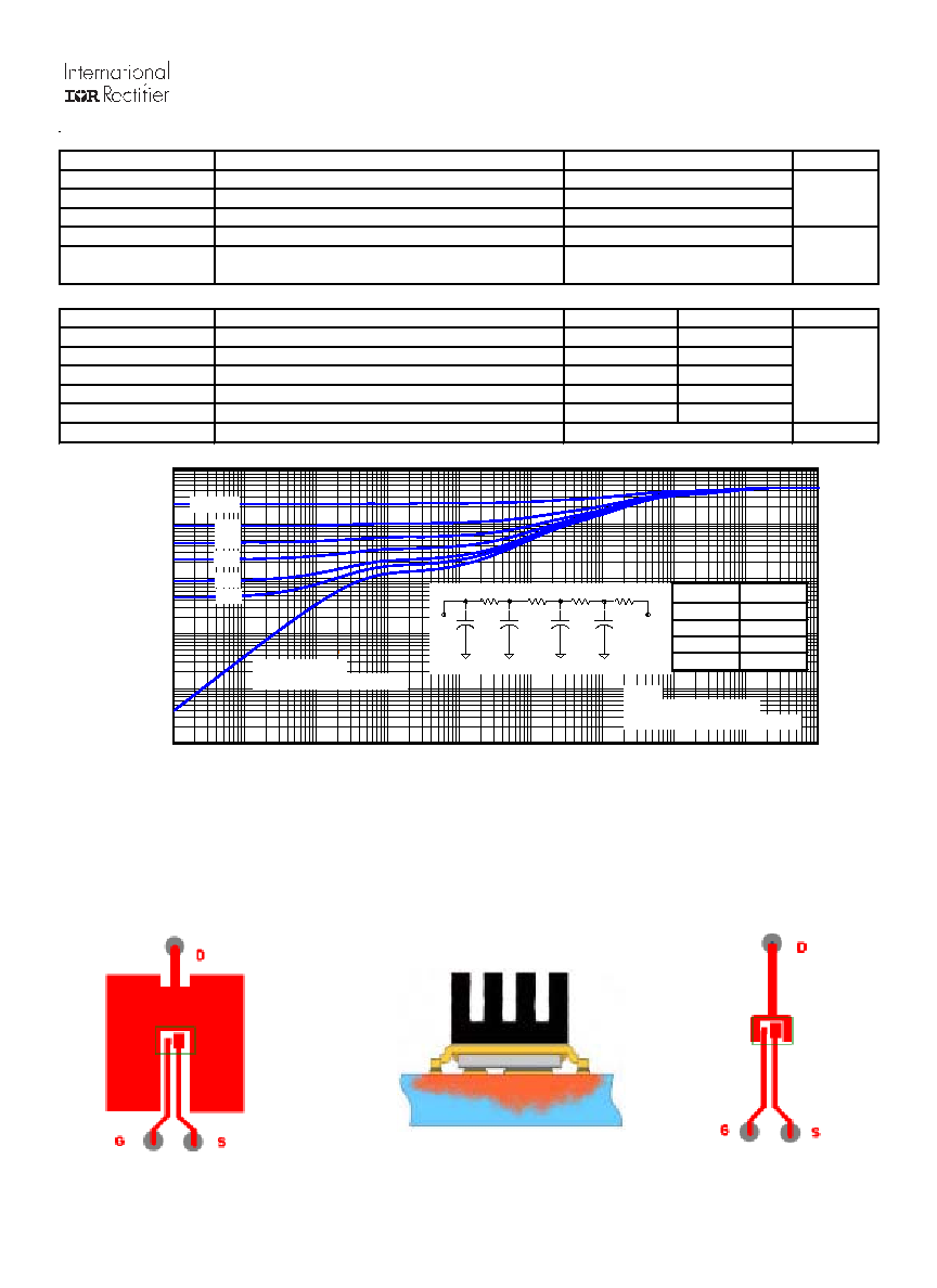
Fig 3. Maximum Effective Transient Thermal Impedance, Junction-to-Ambient
1E-006
1E-005
0.0001
0.001
0.01
0.1
1
10
100
1000
t1 , Rectangular Pulse Duration (sec)
0.001
0.01
0.1
1
10
100
T
h
e
r
m
a
l
R
e
s
p
o
n
s
e
(
Z
t
h
J
A
)
0.20
0.10
D = 0.50
0.02
0.01
0.05
SINGLE PULSE
( THERMAL RESPONSE )
Notes:
1. Duty Factor D = t1/t2
2. Peak Tj = P dm x Zthja + Tc
Ri (°C/W)
i (sec)
1.280114 0.000322
8.725568 0.164798
21.75
2.2576
13.25114
69
J
J
1
1
2
2
3
3
R
1
R
1
R
2
R
2
R
3
R
3
Ci=
i/Ri
Ci=
i/Ri
A
A
4
4
R
4
R
4
Used double sided cooling , mounting pad.
Mounted on minimum footprint full size board with metalized
back and with small clip heatsink.
Notes:
R
is measured at
T
J
of approximately 90°C.
Surface mounted on 1 in. square Cu
(still air).
Mounted to a PCB with
small clip heatsink (still air)
Mounted on minimum
footprint full size board with
metalized back and with small
clip heatsink (still air)
Absolute Maximum Ratings
Parameter
Units
P
D
@T
A
= 25°C
Power Dissipation
e
W
P
D
@T
A
= 70°C
Power Dissipation
e
P
D
@T
C
= 25°C
Power Dissipation
f
T
P
Peak Soldering Temperature
°C
T
J
Operating Junction and
T
STG
Storage Temperature Range
Thermal Resistance
Parameter
Typ.
Max.
Units
R
JA
Junction-to-Ambient
em
45
R
JA
Junction-to-Ambient
km
12.5
R
JA
Junction-to-Ambient
lm
20
°C/W
R
JC
Junction-to-Case
fm
1.4
R
J-PCB
Junction-to-PCB Mounted
1.0
Linear Derating Factor
eÃ
W/°C
0.022
270
-40 to + 150
Max.
89
2.8
1.8
IRF6638PbF
4
www.irf.com
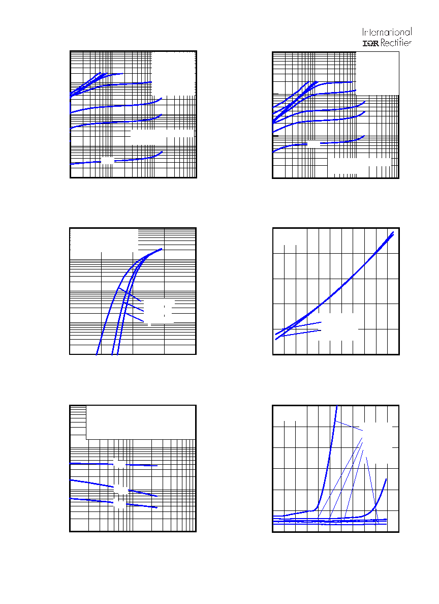
Fig 5. Typical Output Characteristics
Fig 4. Typical Output Characteristics
Fig 6. Typical Transfer Characteristics
Fig 7. Normalized On-Resistance vs. Temperature
Fig 8. Typical Capacitance vs.Drain-to-Source Voltage
Fig 9. Typical On-Resistance Vs.
Drain Current and Gate Voltage
0.1
1
10
100
VDS, Drain-to-Source Voltage (V)
1
10
100
1000
I D
,
D
r
a
i
n
-
t
o
-
S
o
u
r
c
e
C
u
r
r
e
n
t
(
A
)
2.5V
60µs PULSE WIDTH
Tj = 150°C
VGS
TOP
10V
5.0V
4.5V
4.0V
3.5V
3.0V
2.8V
BOTTOM
2.5V
1
2
3
4
5
VGS, Gate-to-Source Voltage (V)
0.1
1
10
100
1000
I D
,
D
r
a
i
n
-
t
o
-
S
o
u
r
c
e
C
u
r
r
e
n
t
(
)
TJ = 150°C
TJ = 25°C
TJ = -40°C
VDS = 15V
60µs PULSE WIDTH
-60 -40 -20 0 20 40 60 80 100 120 140 160
TJ , Junction Temperature (°C)
0.6
0.8
1.0
1.2
1.4
1.6
T
y
p
i
c
a
l
R
D
S
(
o
n
)
(
N
o
r
m
a
l
i
z
e
d
)
ID = 25A
VGS = 10V
VGS = 4.5V
1
10
100
VDS, Drain-to-Source Voltage (V)
100
1000
10000
100000
C
,
C
a
p
a
c
i
t
a
n
c
e
(
p
F
)
VGS = 0V, f = 1 MHZ
Ciss = Cgs + Cgd, C ds SHORTED
Crss = Cgd
Coss = Cds + Cgd
Coss
Crss
Ciss
0 20 40 60 80 100 120 140 160 180 200 220
ID, Drain Current (A)
0
5
10
15
20
25
30
T
y
p
i
c
a
l
R
D
S
(
o
n
)
(
m
)
TJ = 25°C
Vgs = 3.5V
Vgs = 4.0V
Vgs = 4.5V
Vgs = 5.0V
Vgs = 10V
0.1
1
10
100
VDS, Drain-to-Source Voltage (V)
0.1
1
10
100
1000
I D
,
D
r
a
i
n
-
t
o
-
S
o
u
r
c
e
C
u
r
r
e
n
t
(
A
)
VGS
TOP
10V
5.0V
4.5V
4.0V
3.5V
3.0V
2.8V
BOTTOM
2.5V
60µs PULSE WIDTH
Tj = 25°C
2.5V
IRF6638PbF
www.irf.com
5
Fig 13. Typical Threshold Voltage vs. Junction
Temperature
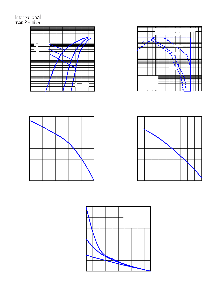
Fig 12. Maximum Drain Current vs. Case Temperature
Fig 10. Typical Source-Drain Diode Forward Voltage
Fig11. Maximum Safe Operating Area
Fig 14. Maximum Avalanche Energy Vs. Drain Current
-75 -50 -25
0
25
50
75 100 125 150
TJ , Temperature ( °C )
1.0
1.5
2.0
2.5
T
y
p
i
c
a
l
V G
S
(
t
h
)
G
a
t
e
t
h
r
e
s
h
o
l
d
V
o
l
t
a
g
e
(
V
)
ID = 250µA
0
1
10
100
VDS, Drain-to-Source Voltage (V)
0.1
1
10
100
1000
I D
,
D
r
a
i
n
-
t
o
-
S
o
u
r
c
e
C
u
r
r
e
n
t
(
A
)
OPERATION IN THIS AREA
LIMITED BY RDS(on)
Tc = 25°C
Tj = 150°C
Single Pulse
100µsec
1msec
10msec
25
50
75
100
125
150
TC , Case Temperature (°C)
0
25
50
75
100
125
150
I D
,
D
r
a
i
n
C
u
r
r
e
n
t
(
A
)
0.1 0.2 0.3 0.4 0.5 0.6 0.7 0.8 0.9 1.0 1.1
VSD, Source-to-Drain Voltage (V)
0
1
10
100
1000
I S
D
,
R
e
v
e
r
s
e
D
r
a
i
n
C
u
r
r
e
n
t
(
A
)
TJ = 150°C
TJ = 25°C
TJ = -40°C
VGS = 0V
25
50
75
100
125
150
Starting TJ , Junction Temperature (°C)
0
25
50
75
100
125
150
E
A
S
,
S
i
n
g
l
e
P
u
l
s
e
A
v
a
l
a
n
c
h
e
E
n
e
r
g
y
(
m
J
)
ID
TOP
5.5A
6.5A
BOTTOM 20A