 | –≠–ª–µ–∫—Ç—Ä–æ–Ω–Ω—ã–π –∫–æ–º–ø–æ–Ω–µ–Ω—Ç: S50L | –°–∫–∞—á–∞—Ç—å:  PDF PDF  ZIP ZIP |

D-670
DISCRETE POWER DIODES and THYRISTORS
DATA BOOK
Next Data Sheet
Index
Previous Datasheet
To Order

SD263C..S50L SERIES
FAST RECOVERY DIODES
Hockey Puk Version
375A
D-671
Bulletin I2071/A
Features
High power FAST recovery diode series
4.5 µs recovery time
High voltage ratings up to 4500V
High current capability
Optimized turn on and turn off characteristics
Low forward recovery
Fast and soft reverse recovery
Press-puk encapsulation
Case style conform to JEDEC DO-200AB (B-PUK)
Maximum junction temperature 125∞C
Typical Applications
Snubber diode for GTO
High voltage free-wheeling diode
Fast recovery rectifier applications
I
F(AV)
375
A
@ T
hs
55
∞C
I
F(RMS)
408
A
I
FSM
@
50Hz
5500
A
@ 60Hz
5760
A
V
RRM
range
3000 to 4500
V
t
rr
4.5
µs
@ T
J
125
∞C
T
J
- 40 to 125
∞C
Parameters
SD263C..S50L
Units
Major Ratings and Characteristics
case style DO-200AB (B-PUK)
Next Data Sheet
Index
Previous Datasheet
To Order

SD263C..S50L Series
D-672
Test conditions
Max. values @ T
J
= 125
∞C
Code
(
µ
s)
(A)
(A/
µ
s)
(V)
(
µ
s)
(
µ
C)
(A)
Recovery Characteristics
S50
5.0
1000
100
- 50
4.5
680
240
(*) di/dt = 25A/us @ T
J
= 25∞C
typical t
rr
I
pk
di/dt (*)
V
r
t
rr
Q
rr
I
rr
@ 25% I
RRM
Square Pulse
@ 25% I
RRM
T
J
= 25
o
C
ELECTRICAL SPECIFICATIONS
Voltage Ratings
Voltage
V
RRM
, maximum repetitive
V
RSM
, maximum non-
I
RRM
max.
Type number
Code
peak reverse voltage
repetitive peak rev. voltage
@ T
J
= T
J
max.
V
V
mA
30
3000
3100
36
3600
3700
40
4000
4100
45
4500
4600
SD263C..S50L
50
I
F(AV)
Max. average forward current
375 (150)
A
180∞ conduction, half sine wave
@ Heatsink temperature
55 (85)
∞C
Double side (single side) cooled
I
F(RMS)
Max. RMS forward current
725
A
@ 25∞C heatsink temperature double side cooled
I
FSM
Max. peak, one-cycle forward,
5500
t = 10ms
No voltage
non-repetitive surge current
5760
t = 8.3ms
reapplied
4630
t = 10ms
50% V
RRM
4850
t = 8.3ms
reapplied
Sinusoidal half wave,
I
2
t
Maximum I
2
t for fusing
151
t = 10ms
No voltage
Initial T
J
= T
J
max.
138
t = 8.3ms
reapplied
107
t = 10ms
50% V
RRM
98
t = 8.3ms
reapplied
I
2
t
Maximum I
2
t for fusing
1510
KA
2
s
t = 0.1 to 10ms, no voltage reapplied
V
F(TO)1
Low level value of threshold
voltage
V
F(TO)2
High level value of threshold
voltage
r
f
1
Low level value of forward
slope resistance
r
f
2
High level value of forward
slope resistance
V
FM
Max. forward voltage drop
3.20
V
I
pk
= 1000A, T
J
= T
J
max, t
p
= 10ms sinusoidal wave
Parameter
SD263C..S50L
Units
Conditions
Forward Conduction
KA
2
s
A
V
m
1.53
(I >
x I
F(AV)
),T
J
= T
J
max.
1.64
(16.7% x
x I
F(AV)
< I <
x I
F(AV)
), T
J
= T
J
max.
1.71
(I >
x I
F(AV)
),T
J
= T
J
max.
1.56
(16.7% x
x I
F(AV)
< I <
x I
F(AV)
), T
J
= T
J
max.
To Order
Next Data Sheet
Index
Previous Datasheet
SD263C..S50L Series
D-675
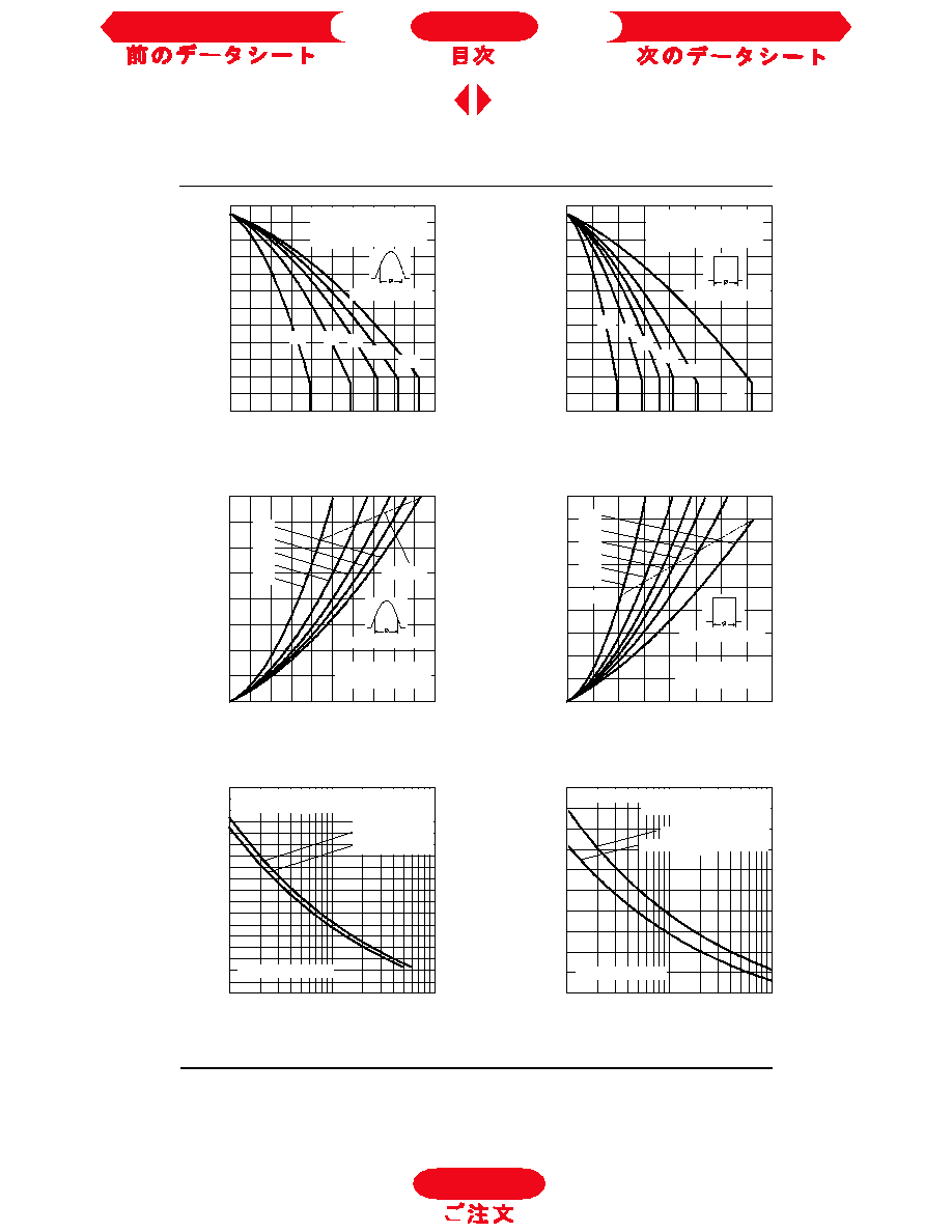
Fig. 3 - Current Ratings Characteristics
Fig. 4 - Current Ratings Characteristics
Fig. 5 - Forward Power Loss Characteristics
Fig. 6 - Forward Power Loss Characteristics
Fig. 7 - Maximum Non-repetitive Surge Current
Single and Double Side Cooled
Fig. 8 - Maximum Non-repetitive Surge Current
Single and Double Side Cooled
To Order
Next Data Sheet
Index
Previous Datasheet

SD263C..S50L Series
D-676
Fig. 10 - Thermal Impedance Z
thJ-hs
Characteristic
Fig. 9 - Forward Voltage Drop Characteristics
Fig. 11 - Typical Forward Recovery Characteristics
Fig. 12 - Recovery Time Characteristics
Fig. 13 - Recovery Charge Characteristics
Fig. 14 - Recovery Current Characteristics
To Order
Next Data Sheet
Index
Previous Datasheet

SD263C..S50L Series
D-677
Fig. 18 - Frequency Characteristics
Fig. 20 - Frequency Characteristics
Fig. 17 - Maximum Total Energy Loss Per Pulse Characteristics
Fig. 19 - Maximum Total Energy Loss Per Pulse Characteristics
Fig. 15 - Maximum Total Energy Loss Per Pulse Characteristics
Fig. 16 - Frequency Characteristics
To Order
Next Data Sheet
Index
Previous Datasheet

SD263C..S50L Series
D-673
180∞
0.012
0.011
0.008
0.008
T
J
= T
J
max.
120∞
0.014
0.015
0.014
0.014
90∞
0.018
0.018
0.019
0.019
K/W
60∞
0.026
0.027
0.027
0.028
30∞
0.045
0.046
0.046
0.046
T
J
Max. junction operating temperature range
-40 to 125
T
stg
Max. storage temperature range
-40 to 150
R
thJ-hs
Max. thermal resistance,
0.11
DC operation single side cooled
junction to heatsink
0.05
DC operation double side cooled
F
Mounting force, ± 10%
9800
N
(1000)
(Kg)
wt
Approximate weight
230
g
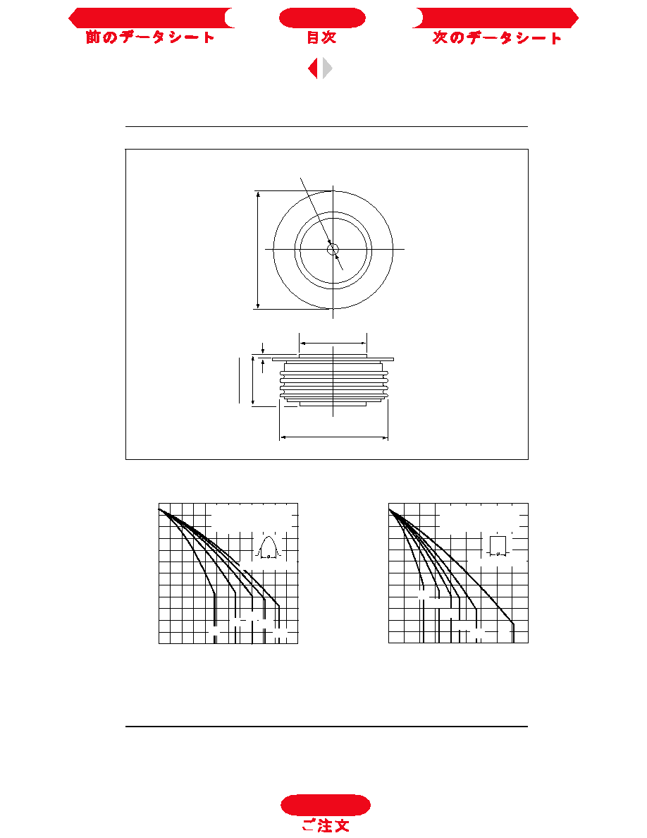
Case style
DO-200AB (B-PUK)
See outline table
Parameter
SD263C..S50L
Units
Conditions
Thermal and Mechanical Specifications
∞C
Ordering Information Table
1
-
Diode
2
-
Essential part number
3
-
3 = Fast recovery
4
-
C = Ceramic Puk
5
-
Voltage code: Code x 100 = V
RRM
(See Voltage Ratings table)
6
-
t
rr
code
7
-
L = Puk Case DO-200AB (B-PUK)
SD
26
3
C
45 S50
L
1
2
3
4
5
6
7
Device Code
K/W
Conduction angle
Units
Conditions
Single Side Double Side
Single Side Double Side
Sinusoidal conduction
Rectangular conduction
R
thJ-hs
Conduction
(The following table shows the increment of thermal resistence R
thJ-hs
when devices operate at different conduction angles than DC)
To Order
Next Data Sheet
Index
Previous Datasheet
SD263C..S50L Series
D-674
Outline Table
Fig. 2 - Current Ratings Characteristics
Fig. 1 - Current Ratings Characteristics
BOTH ENDS
0.8 (0.03)
TWO PLACES
3.5(0.14) DIA. NOM. x
1.8(0.07) DEEP MIN.
34 (1.34) DIA. MAX.
5
8
.
5
(
2
.
3
0
)
D
I
A
.
M
A
X
.
2
6
.
9
(
1
.
0
6
)
2
5
.
4
(
1
)
BOTH ENDS
53 (2.09) DIA. MAX.
Conforms to JEDEC DO-200AB (B-PUK)
All dimensions in millimeters (inches)
To Order
Next Data Sheet
Index
Previous Datasheet