Äîêóìåíòàöèÿ è îïèñàíèÿ www.docs.chipfind.ru
200A
FAST RECOVERY DIODES
Stud Version
SD203N/R SERIES
1
Bulletin I2064 rev. A 09/94
www.irf.com
Features
High power FAST recovery diode series
1.0 to 2.0 µs recovery time
High voltage ratings up to 2500V
High current capability
Optimized turn on and turn off characteristics
Low forward recovery
Fast and soft reverse recovery
Compression bonded encapsulation
Stud version JEDEC DO-205AB (DO-9)
Maximum junction temperature 125°C
Typical Applications
Snubber diode for GTO
High voltage free-wheeling diode
Fast recovery rectifier applications
I
F(AV)
200
A
@ T
C
85
°C
I
F(RMS)
314
A
I
FSM
@
50Hz
4990
A
@ 60Hz
5230
A
I
2
t
@
50Hz
125
KA
2
s
@ 60Hz
114
KA
2
s
V
RRM
range
400 to 2500
V
t
rr
range
1.0 to 2.0
µs
@ T
J
25
°C
T
J
- 40 to 125
°C
Parameters
SD203N/R
Units
Major Ratings and Characteristics
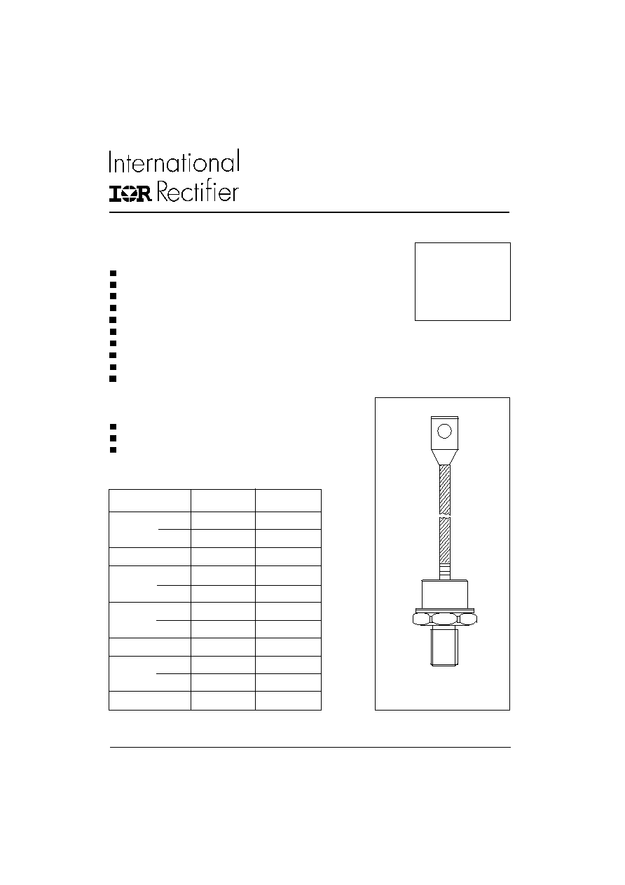
case style
DO-205AB (DO-9)
SD203N/R Series
2
www.irf.com
Bulletin I2064 rev. A 09/94
ELECTRICAL SPECIFICATIONS
Voltage Ratings
Voltage
V
RRM
max. repetitive
V
RSM
, maximum non-
I
RRM
max.
Type number
Code
peak and off-state voltage
repetitive peak voltage
T
J
= 125°C
V
V
mA
04
400
500
SD203N/R..S10
08
800
900
10
1000
1100
12
1200
1300
SD203N/R..S15
14
1400
1500
16
1600
1700
20
2000
2100
25
2500
2600
SD203N/R..S20
I
F(AV)
Max. average forward current
200
A
180° conduction, half sine wave.
@ Case temperature
85
°C
I
F(RMS)
Max. RMS current
314
A
DC @ 76°C case temperature
I
FSM
Max. peak, one-cycle
4990
t = 10ms
No voltage
non-repetitive forward current
5230
t = 8.3ms
reapplied
4200
t = 10ms
100% V
RRM
4400
t = 8.3ms
reapplied
Sinusoidal half wave,
I
2
t
Maximum I
2
t for fusing
125
t = 10ms
No voltage
Initial T
J
= T
J
max.
114
t = 8.3ms
reapplied
88
t = 10ms
100% V
RRM
81
t = 8.3ms
reapplied
I
2
t
Maximum I
2
t for fusing
1250
KA
2
s
t = 0.1 to 10ms, no voltage reapplied
V
F(TO)1
Low level of threshold voltage
1.00
(16.7% x
x I
F(AV)
< I <
x I
F(AV)
), T
J
= T
J
max.
V
F(TO)
2
High level of threshold voltage
1.47
(I >
x I
F(AV)
), T
J
= T
J
max.
r
f1
Low level of forward slope resistance
1.10
(16.7% x
x I
F(AV)
< I <
x I
F(AV)
), T
J
= T
J
max.
r
f2
High level of forward slope resistance
0.46
(I >
x I
F(AV)
), T
J
= T
J
max.
V
FM
Max. forward voltage
1.65
V
I
pk
= 628A, T
J
= 25°C, t
p
= 400 µs square pulse
Parameter
SD203N/R
Units
Conditions
Forward Conduction
KA
2
s
A
m
V
Test conditions
Max. values @ T
J
= 125
°C
Recovery Characteristics
typical t
rr
I
pk
di/dt
V
r
t
rr
Q
rr
I
rr
@ 25% I
RRM
Square Pulse
@ 25% I
RRM
T
J
= 25
o
C
S10
1.0
2.4
52
33
S15
1.5
2.9
90
44
S20
2.0
3.2
107
46
750
25
- 30
Code
(
µ
s)
(A)
(A/
µ
s)
(V)
(
µ
s)
(
µ
C)
(A)
35
SD203N/R Series
3
www.irf.com
Bulletin I2064 rev. A 09/94
Thermal and Mechanical Specification
Parameter
SD203N/R
Units
Conditions
°C
K/W
Nm
T
J
Max. operating temperature range
-40 to 125
T
stg
Max. storage temperature range
-40 to 150
R
thJC
Max. thermal resistance, junction to case
0.115
DC operation
R
thCS
Max. thermal resistance, case to heatsink
0.08
Mounting surface, smooth, flat and greased
T
Mounting torque ±10%
31
Not lubricated threads
24.5
Lubricated threads
wt
Approximate weight
250
g
Case style
DO-205AB (DO-9)
See Outline Table
R
thJC
Conduction
(The following table shows the increment of thermal resistence R
thJC
when devices operate at different conduction angles than DC)
180°
0.010
0.008
T
J
= T
J
max.
120°
0.013
0.014
90°
0.017
0.019
K/W
60°
0.025
0.027
30°
0.044
0.044
Conduction angle
Sinusoidal conduction
Rectangular conduction Units
Conditions
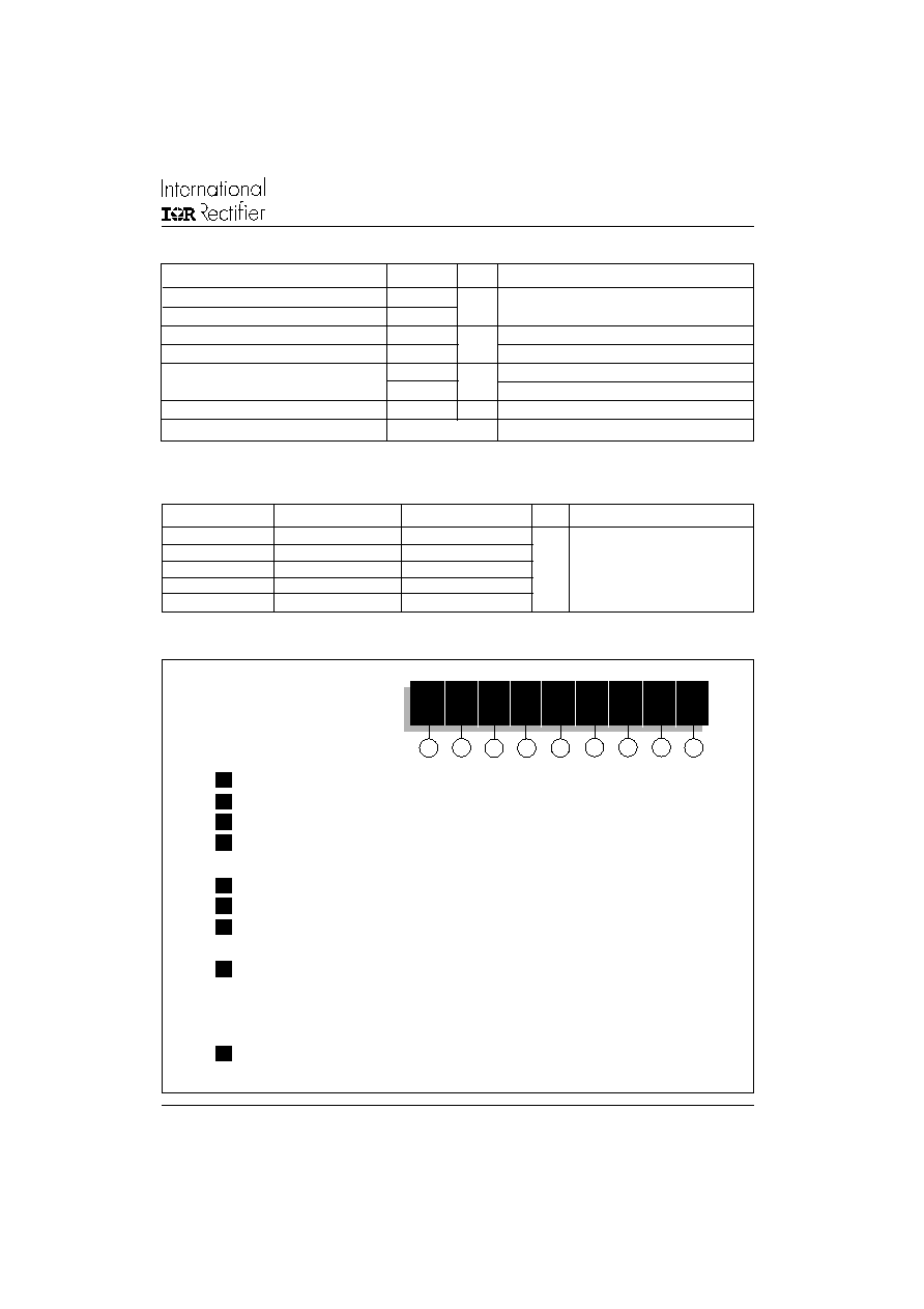
Ordering Information Table
1
-
Diode
2
-
Essential part number
3
-
3 = Fast recovery
4
-
N = Stud Normal Polarity (Cathode to Stud)
R = Stud Reverse Polarity (Anode to Stud)
5
-
Voltage code: Code x 100 = V
RRM
(see Voltage Ratings table)
6
-
t
rr
code (see Recovery Characteristics table)
7
-
P = Stud base DO-205AB (DO-9) 3/4" 16UNF-2A
M = Stud base DO-205AB (DO-9) M16 X 1.5
8
-
7
B = Flag top terminals (for Cathode/ Anode Leads)
S = Isolated lead with silicone sleeve
(Red = Reverse Polarity; Blue = Normal Polarity)
None = Not isolated lead
9
-
C = Ceramic housing (over 1600V)
V = Glass-metal seal (only up to 1600V)
5
1
2
3
4
SD
20
3
R
25
S20
P
B
C
7
6
8
9
Device Code
SD203N/R Series
4
www.irf.com
Bulletin I2064 rev. A 09/94
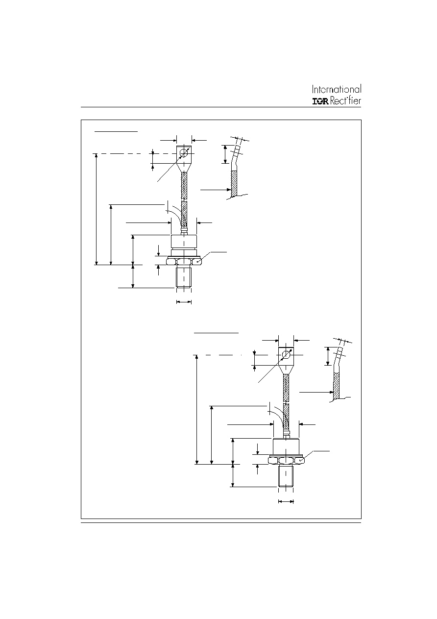
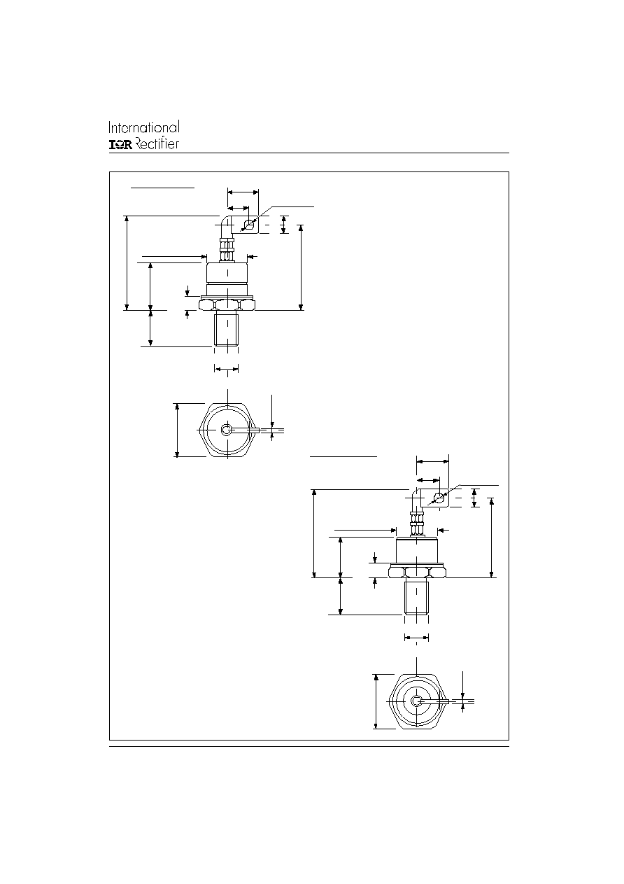
Outline Table
Conform to JEDEC DO-205AB (DO-9)
All dimensions in millimeters (inches)
M
AX.
CERAMIC HOUSING
MAX.
MA
X
.
21 (
0
.
82)
MA
X
.
19 (0.75)
9.5 (
0
.
3
7
)
MIN
.
DIA. 8.5 (0.33) NOM.
82 (
3
.23)
MIN
.
DIA. 27.5 (1.08) MAX.
38 (
1
.5
0)
16 (
0
.
63)
SW 32
* FOR METRIC DEVICE: M16 X 1.5
21
0 (
8
.27)
±
10 (
0
.3
9)
3/4"-16UNF-2A*
C.S. 35mm
4 (0.16) MAX.
3
9
(
1
.53)
MA
X
.
2
(0.054 s.i.)
MA
X
.
GLASS-METAL SEAL
MAX.
MA
X
.
21
(
0
.
8
2
)
MA
X
.
19 (0.75)
9.
5 (
0
.
3
7)
M
I
N
.
DIA. 8.5 (0.33) NOM.
75 (
2
.
9
5
)
M
I
N
.
DIA. 28.5 (1.08) MAX.
28
.
5
(
1
.
1
2)
16
(
0
.
63)
SW 32
* FOR METRIC DEVICE: M16 X 1.5
20
0 (
7
.
87)
±
10
(
0
.
3
9
)
3/4-16UNF-2A*
C.S. 35mm
4 (0.16) MAX.
39
(
1
.
5
3)
M
AX.
2
(0.054 s.i.)
SD203N/R Series
5
www.irf.com
Bulletin I2064 rev. A 09/94
Outline Table
DO-205AB (DO-9) Flag
All dimensions in millimeters (inches)
MA
X
.
GLASS-METAL SEAL
MA
X
.
2
1
(
0
.
83)
MA
X
.
DIA. 28.5 (1.12) MAX.
28.
5 (
1
.
12)
16 (
0
.
63)
21 (0.83)
14 (0.55)
DIA. 6.5 (0.26)
3 (
0
.
1
2
)
32 (
1
.
26)
3/4"-16UNF-2A*
*FOR METRIC DEVICE: M16 X 1.5
7
0
(
2
.7
5
)
M
A
X
.
13 (
0
.
51)
62 (
2
.
4
4)
M
AX.
CERAMIC HOUSING
2
1
(
0
.
82)
MA
X
.
38 (
1
.
50)
3 (
0
.
1
2
)
32 (
1
.
2
6
)
79
(
3
.
11)
M
A
X
.
21 (0.83)
DIA. 6.5 (0.25)
13 (
0
.
51)
DIA. 27.5 (1.08) MAX.
72 (
2
.
8
3
)
3/4"-16UNF-2A*
*FOR METRIC DEVICE. M16 X 1.5
14 (0.55)
1
6
(
0
.
63)
M
AX.