250A
FAST RECOVERY DIODES
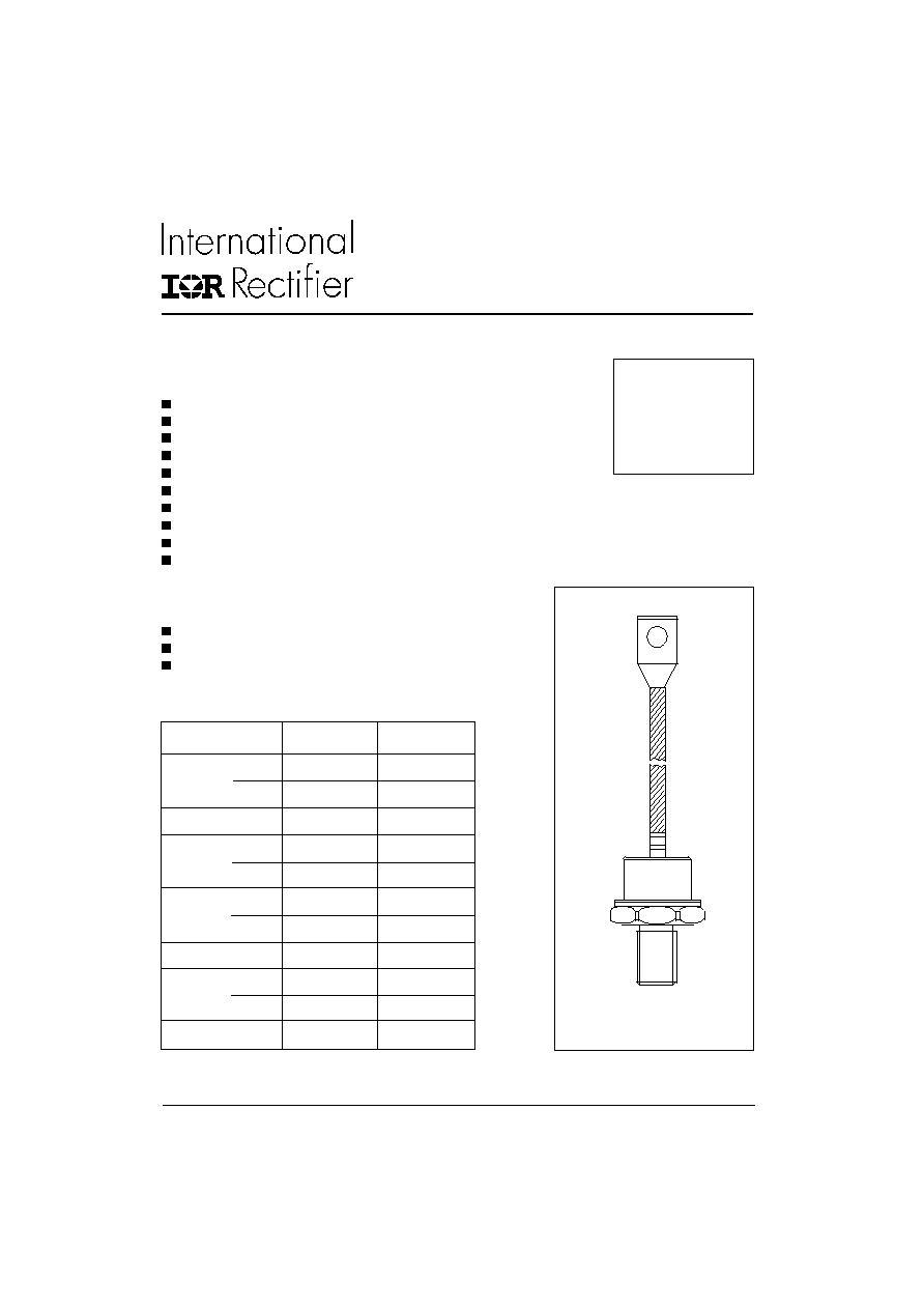
Stud Version
SD253N/R SERIES
1
Bulletin I2065 rev. A 09/94
www.irf.com
Features
High power FAST recovery diode series
1.5 to 2.0 µs recovery time
High voltage ratings up to 1600V
High current capability
Optimized turn on and turn off characteristics
Low forward recovery
Fast and soft reverse recovery
Compression bonded encapsulation
Stud version JEDEC DO-205AB (DO-9)
Maximum junction temperature 125∞C
Typical Applications
Snubber diode for GTO
High voltage free-wheeling diode
Fast recovery rectifier applications
I
F(AV)
250
A
@ T
C
85
∞C
I
F(RMS)
392
A
I
FSM
@
50Hz
5350
A
@ 60Hz
5600
A
I
2
t
@
50Hz
143
KA
2
s
@ 60Hz
130
KA
2
s
V
RRM
range
400 to 1600
V
t
rr
range
1.5 to 2.0
µs
@ T
J
25
∞C
T
J
- 40 to 125
∞C
Parameters
SD253N/R
Units
Major Ratings and Characteristics
case style
DO-205AB (DO-9)
SD253N/R Series
2
www.irf.com
Bulletin I2065 rev. A 09/94
I
F(AV)
Max. average forward current
250
A
180∞ conduction, half sine wave.
@ Case temperature
85
∞C
I
F(RMS)
Max. RMS current
392
A
DC @ 74∞C case temperature
I
FSM
Max. peak, one-cycle
5350
t = 10ms
No voltage
non-repetitive forward current
5600
t = 8.3ms
reapplied
4500
t = 10ms
100% V
RRM
4710
t = 8.3ms
reapplied
Sinusoidal half wave,
I
2
t
Maximum I
2
t for fusing
143
t = 10ms
No voltage
Initial T
J
= T
J
max.
130
t = 8.3ms
reapplied
101
t = 10ms
100% V
RRM
92
t = 8.3ms
reapplied
I
2
t
Maximum I
2
t for fusing
1430
KA
2
s
t = 0.1 to 10ms, no voltage reapplied
V
F(TO)1
Low level of threshold voltage
0.87
(16.7% x
x I
F(AV)
< I <
x I
F(AV)
), T
J
= T
J
max.
V
F(TO)
2
High level of threshold voltage
1.17
(I >
x I
F(AV)
), T
J
= T
J
max.
r
f1
Low level of forward slope resistance
0.62
(16.7% x
x I
F(AV)
< I <
x I
F(AV)
), T
J
= T
J
max.
r
f2
High level of forward slope resistance
0.29
(I >
x I
F(AV)
), T
J
= T
J
max.
V
FM
Max. forward voltage
1.38
V
I
pk
= 785A, T
J
= 25∞C, t
p
= 400 µs square pulse
ELECTRICAL SPECIFICATIONS
Voltage Ratings
Parameter
SD253N/R
Units
Conditions
Forward Conduction
KA
2
s
A
m
V
Voltage
V
RRM
max. repetitive
V
RSM
, maximum non-
I
RRM
max.
Type number
Code
peak and off-state voltage
repetitive peak voltage
T
J
= 125∞C
V
V
mA
04
400
500
SD253N/R..S15
08
800
900
10
1000
1100
12
1200
1300
SD253N/R..S20
14
1400
1500
16
1600
1700
Test conditions
Max. values @ T
J
= 125
∞C
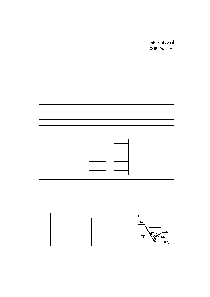
Recovery Characteristics
typical t
rr
I
pk
di/dt
V
r
t
rr
Q
rr
I
rr
@ 25% I
RRM
Square Pulse
@ 25% I
RRM
T
J
= 25
o
C
750
25
- 30
Code
(
µ
s)
(A)
(A/
µ
s)
(V)
(
µ
s)
(
µ
C)
(A)
S15
1.5
2.9
90
44
S20
2.0
3.2
107
46
35

SD253N/R Series
3
www.irf.com
Bulletin I2065 rev. A 09/94
Thermal and Mechanical Specification
Parameter
SD253N/R
Units
Conditions
∞C
T
J
Max. operating temperature range
-40 to 125
T
stg
Max. storage temperature range
-40 to 150
R
thJC
Max. thermal resistance, junction to case
0.115
DC operation
R
thCS
Max. thermal resistance, case to heatsink
0.08
Mounting surface, smooth, flat and greased
T
Mounting torque ± 10%
31
Not lubricated threads
24.5
Lubricated threads
wt
Approximate weight
250
g
Case style
DO-205AB (DO-9)
See Outline Table
K/W
Nm
R
thJC
Conduction
(The following table shows the increment of thermal resistence R
thJC
when devices operate at different conduction angles than DC)
180∞
0.010
0.008
T
J
= T
J
max.
120∞
0.013
0.014
90∞
0.017
0.019
K/W
60∞
0.025
0.027
30∞
0.044
0.044
Conduction angle
Sinusoidal conduction
Rectangular conduction Units
Conditions
1
-
Diode
2
-
Essential part number
3
-
3 = Fast recovery
4
-
N = Stud Normal Polarity (Cathode to Stud)
R = Stud Reverse Polarity (Anode to Stud)
5
-
Voltage code: Code x 100 = V
RRM
(see Voltage Ratings table)
6
-
t
rr
code (see Recovery Characteristics table)
7
-
P = Stud base DO-205AB (DO-9) 3/4" 16UNF-2A
M = Stud base DO-205AB (DO-9) M16 X 1.5
8
-
7
B = Flag top terminals (for Cathode/ Anode Leads)
S = Isolated lead with silicone sleeve
(Red = Reverse Polarity; Blue = Normal Polarity)
None = Not isolated lead
9
-
V = Glass-metal seal
5
1
2
3
4
SD
25
3
R
16
S20
P
B
V
7
6
8
9
Device Code
Ordering Information Table

SD253N/R Series
4
www.irf.com
Bulletin I2065 rev. A 09/94
Outline Table
DO-205AB (DO-9) Flag
All dimensions in millimeters (inches)
Conform to JEDEC DO-205AB (DO-9)
All dimensions in millimeters (inches)
M
AX.
GLASS-METAL SEAL
MAX.
M
AX.
21
(
0
.
8
2)
M
AX.
19 (0.75)
9.
5
(
0
.
37)
M
I
N
.
DIA. 8.5 (0.33) NOM.
75 (
2
.
9
5
)
M
I
N
.
DIA. 28.5 (1.08) MAX.
28
.
5
(
1
.
1
2)
16 (
0
.
6
3)
SW 32
* FOR METRIC DEVICE: M16 X 1.5
20
0 (
7
.
87)
±
1
0
(
0
.
39)
3/4-16UNF-2A*
C.S. 35mm
4 (0.16) MAX.
39 (
1
.
5
3)
MA
X
.
2
(0.054 s.i.)
M
AX.
GLASS-METAL SEAL
M
AX.
21
(
0
.
8
3)
M
AX.
DIA. 28.5 (1.12) MAX.
2
8
.
5
(
1
.1
2
)
16 (
0
.
63)
21 (0.83)
14 (0.55)
DIA. 6.5 (0.26)
3 (
0
.
1
2
)
32 (
1
.
26)
3/4"-16UNF-2A*
*FOR METRIC DEVICE: M16 X 1.5
70 (
2
.
7
5
)
M
A
X
.
13 (
0
.
51)
62
(
2
.
4
4)

SD253N/R Series
5
www.irf.com
Bulletin I2065 rev. A 09/94
Fig. 1 - Current Ratings Characteristics
Fig. 2 - Current Ratings Characteristics
Fig. 3 - Forward Power Loss Characteristics
Fig. 4 - Forward Power Loss Characteristics
Fig. 5 - Maximum Non-repetitive Surge Current
Fig. 6 - Maximum Non-repetitive Surge Current
80
90
100
110
120
130
0
50
100
150
200
250
300
30∞
60∞
90∞
120∞
180∞
Average Forward Current (A)
Conduction Angle
M
a
x
i
m
u
m
A
l
l
o
w
a
bl
e
C
a
se
T
e
m
pe
r
a
t
u
r
e
(
∞C
)
SD253N/R Series
R (DC) = 0.115 K/W
thJC
70
80
90
100
110
120
130
0
100
200
300
400
DC
30∞
60∞
90∞
120∞
180∞
Conduction Period
M
a
x
i
m
u
m
A
l
low
a
b
l
e C
a
s
e
Tem
p
er
a
t
u
r
e
(
∞C
)
Average Forward Current (A)
SD253N/R Series
R (DC) = 0.115 K/W
thJC
0
50
100
150
200
250
300
350
0
50
100
150
200
250
180∞
120∞
90∞
60∞
30∞
RMS Limit
Conduction Angle
M
a
x
i
m
u
m
A
v
e
r
ag
e
F
o
r
w
ar
d
P
o
we
r
Lo
ss (
W
)
Average Forward Current (A)
SD253N/R Series
T = 125∞C
J
0
50
100
150
200
250
300
350
400
450
500
0
100
200
300
400
DC
180∞
120∞
90∞
60∞
30∞
RMS Limit
Conduction Period
M
a
x
i
m
u
m
A
v
e
r
ag
e
F
o
r
w
ar
d P
o
w
e
r
L
o
ss (
W
)
Average Forward Current (A)
SD253N/R Series
T = 125∞C
J
1000
2000
3000
4000
5000
6000
0.01
0.1
1
Pulse Train Duration (s)
P
e
a
k
Hal
f
S
i
ne
W
a
v
e
F
o
r
w
ar
d
C
u
r
r
e
n
t
(
A
)
Versus Pulse Train Duration.
Maximum Non Repetitive Surge Current
Initial T = 125∞C
No Volt age Reapplied
Rated V Reapplied
RRM
J
SD253N/R Series
1000
1500
2000
2500
3000
3500
4000
4500
5000
1
10
100
Number Of Equal Amplitude Half Cycle Current Pulses (N)
P
e
ak
Hal
f
S
i
n
e
W
a
v
e
F
o
r
w
ar
d
C
u
r
r
e
n
t
(
A
)
Initial T = 125∞C
@ 60 Hz 0.0083 s
@ 50 Hz 0.0100 s
J
SD253N/R Series
At Any Rated Load Condition And With
Rated V Applied Following Surge.
RRM

SD253N/R Series
6
www.irf.com
Bulletin I2065 rev. A 09/94
Fig. 8 - Thermal Impedance Z
thJC
Characteristic
Fig. 7 - Forward Voltage Drop Characteristics
Fig. 9 - Recovery Time Characteristics
Fig. 10 - Recovery Charge Characteristics
Fig. 11 - Recovery Current Characteristics
Fig. 14 - Recovery Current Characteristics
Fig. 13 - Recovery Charge Characteristics
Fig. 12 - Recovery Time Characteristics
1
10
100
1000
10000
0
1
2
3
4
I
n
s
t
an
t
a
n
e
o
u
s
F
o
r
w
ar
d C
u
r
r
e
n
t
(
A
)
Instantaneous Forward Voltage (V)
SD253N/R Series
T = 25 ∞C
J
T = 125 ∞C
J
0.001
0.01
0.1
1
0.001
0.01
0.1
1
10
Square Wave Pulse Duration (s)
th
J
C
Tr
a
n
s
i
en
t
Th
er
m
a
l
I
m
p
e
d
a
n
c
e
Z
(
K
/
W
)
Steady State Value:
R = 0.1 15K/W
(DC Operation)
thJC
SD253N/R Series
10
20
30
40
50
60
70
80
90
100
110
120
130
10 20 30 40 50 60 70 80 90 100
M
a
x
i
m
u
m
R
e
v
e
rs
e
R
e
c
o
v
e
ry
C
u
rr
e
n
t
-
Irr
(
A
)
Rate Of Fall Of Forward Current - di/dt (A/µs)
400 A
200 A
I = 750 A
Square Pulse
FM
SD253N/R..S15 Series
T = 125 ∞C, V = 30V
J
r
50
60
70
80
90
100
110
120
130
140
150
160
170
10 20 30 40 50 60 70 80 90 100
M
a
x
i
m
u
m
R
e
ve
r
s
e
R
e
c
o
ve
r
y
C
h
a
r
g
e
-
Q
r
r
(
µC
)
Rate Of Fall Of Forward Current - di/dt (A/µs)
400 A
200 A
I = 750 A
Square Pulse
FM
SD253N/R..S15 Series
T = 125 ∞C, V = 30V
J
r
1.6
2
2.4
2.8
3.2
3.6
10
100
Rate Of Fall Of Forward Current - di/dt (A/µs)
M
a
x
i
m
u
m
Re
v
e
r
s
e
R
e
c
o
v
e
ry
T
i
m
e
-
T
rr (
µs
)
400 A
200 A
I = 750 A
Square Pulse
FM
SD253N/R..S15 Series
T = 125 ∞C, V = 30V
r
J
20
30
40
50
60
70
80
90
100
110
120
130
10 20 30 40 50 60 70 80 90 100
M
a
x
i
m
u
m
R
e
v
e
r
s
e
R
e
c
o
v
e
ry
C
u
rre
n
t
-
Irr
(
A
)
Rate Of Fall Of Forward Current - di/dt (A/µs)
400 A
200 A
I = 750 A
Square Pulse
FM
SD253N/R..S20 Series
T = 125 ∞C, V = 30V
J
r
50
100
150
200
250
300
10 20 30 40 50 60 70 80 90 100
M
a
x
i
m
u
m
R
e
v
e
rs
e
R
e
c
o
v
e
r
y
C
h
a
r
ge
-
Q
rr
(
µC
)
Rate Of Fall Of Forward Current - di/dt (A/µs)
400 A
200 A
I = 750 A
Square Pulse
FM
SD253N/R..S20 Series
T = 125 ∞C, V = 30V
J
r
2.4
2.6
2.8
3
3.2
3.4
3.6
10
100
Rate Of Fall Of Forward Current - di/dt (A/µs)
M
a
x
i
m
u
m
Re
v
e
r
s
e
R
e
c
o
v
e
ry
T
i
m
e
-
T
rr (
µs
)
400 A
200 A
I = 750 A
Square Pulse
FM
SD253N/R..S20 Series
T = 125 ∞C, V = 30V
J
r

SD253N/R Series
7
www.irf.com
Bulletin I2065 rev. A 09/94
Fig. 16 - Maximum Total Energy Loss Per Pulse Characteristics
Fig. 15 - Maximum Total Energy Loss Per Pulse Characteristics
1E1
1E2
1E3
1E4
1E1
1E2
1E3
1E4
1
2
0.1
Pulse Basewidth (µs)
P
e
ak
F
o
rwar
d
C
u
rre
n
t
(
A
)
4
dv/dt = 1000V/µs
Sinusoidal Pulse
20 joules per pulse
10
0.4
0.2
0.04
T = 125∞C, V = 800V
J
RRM
0.02
0.01
SD253N/R..S15 Series
1E4
tp
1E1
1E2
1E3
1E4
1
2
0.1
Pulse Basewidth (µs)
4
20 jo ules per pulse
10
0.4
0.2
T = 125∞C, V = 800V
J
RRM
Trapezoidal Pulse
dv/dt = 1000V/µs; di/dt=50A/µs
SD253N/R.. S15 Series
tp
1E1
1E1
1E2
1E3
1E4
1E1
1E2
1E3
1E4
1
2
0.1
Pulse Basewidth (µs)
P
e
ak
F
o
r
w
a
r
d
C
u
r
r
e
nt
(
A
)
4
dv/dt = 1000 V/µs
Sinusoidal Pulse
20 joules per pulse
10
0.4
0.2
0.04
0.02
0.01
T = 125∞C, V = 1120V
J
RRM
SD253N/R..S20 Series
1E4
tp
1E1
1E2
1E3
1E4
1
2
Pulse Basewidth (µs)
4
20 joules per pulse
10
0.4
0.2
Trapezoidal Pulse
dv/dt = 1000V/µs; di/dt=50A/µs
SD253N/R.. S20 Series
T = 125∞C, V = 1120V
J
RRM
tp
1E1