Parameter
Description
Min
Typ.
Max
Test Conditions
V
(BR)DSS
Drain-to-Source Breakdown Voltage
75V
≠≠≠
≠≠≠
V
GS
= 0V, I
D
= 250µA
R
DS(on)***
Static Drain-to-Source On-Resistance
≠≠≠
2.5m
4.5m
V
GS
= 10V, I
D
= 110A
V
GS(th)
Gate Threshold Voltage
2.0
≠≠≠
4.0V
V
DS
= V
GS
, I
D
= 250µA
I
DSS
Drain-to-Source Leakage Current
≠≠≠
≠≠≠
20µA
V
DS
= 75V, V
GS
= 0V, T
J
= 25∞C
I
GSS
Gate-to-Source Leakage Current
≠≠≠
≠≠≠
± 200nA
V
GS
= ±20V
T
J
Operating Junction and
-55∞C to 175∞C Max.
T
STG
Storage Temperature Range
Nominal Back Metal Composition, Thickness:
Cr-NiV-Ag ( 1kA∞-2kA∞-5kA∞ )
Nominal Front Metal Composition, Thickness:
100% Al (0.008 mm)
Dimensions:
.257" x .360" [ 6.53 mm x 9.14 mm ]
Wafer Diameter:
150 mm, with 100 flat
Wafer Thickness:
0.254 mm ± 0.025 mm
Relevant Die Mechanical Drawing Number
01-5403
Minimum Street Width
0.107 mm
Reject Ink Dot Size
0.51 mm Diameter Minimum
Recommended Storage Environment:
Store in original container, in dessicated
nitrogen, with no contamination
Recommended Die Attach Conditions:
For optimum electrical results, die attach
temperature should not exceed 300 ∞C
Reference Packaged Part
IRFP2907
75V
R
DS(on)
= 2.5m
(
typ.)
6" Wafer
10/4/00
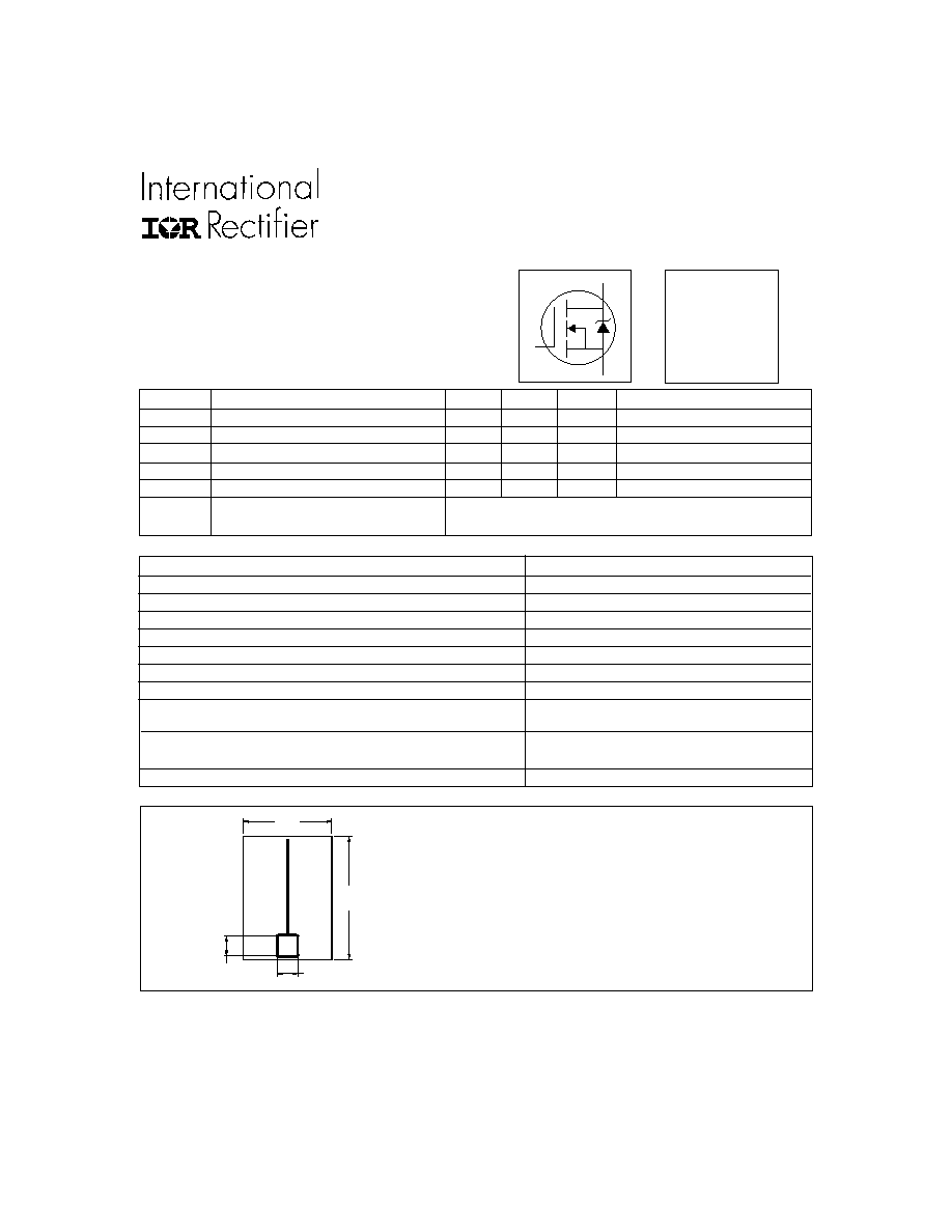
Mechanical Data
Die Outline
Electrical Characteristics *
IRFC2907B
HEXFET
Æ
Power MOSFET Die in Wafer Form
S
D
G
www.irf.com
1
GAT E
SOURCE
SOURCE
6.53
[.257]
9.14
[.360]
0.508
[.020]
0.508
[.020]
5. UNL ES S OT HERWIS E NOT ED AL L DIE ARE GEN III
< 1.270 T OL ERANCE = + /- 0.102
< [.050] T OL ERANCE = + /- [.004]
> 1.270 T OL ERANCE = + /- 0.203
> [.050] T OL ERANCE = + /- [.008]
L ENGT H
OVERALL DIE:
WIDTH
&
NOT ES :
2. CONT ROL L ING DIMENS ION: [INCH].
3. LET T ER DES IGNAT ION:
4. DIMENS IONAL T OL ERANCES:
1. AL L DIMENS IONS ARE S HOWN IN MILL IMET ERS [INCHES ].
< 0.635 T OL ERANCE = + /- 0.013
< [.0250] T OLERANCE = + /- [.0005]
> 0.635 T OL ERANCE = + /- 0.025
> [.0250] T OLERANCE = + /- [.0010]
IS = CURRENT S ENS E
S K = S OU RCE K ELVIN
B ONDING PADS :
WIDTH
L ENGT H
&
S = S OURCE
G = GAT E
E = EMITT ER
* Electrical characteristics are reported for the reference packaged part (see above) and can not be guaranteed in
die sales form. Variations in customer packaging materials, dimensions and processes may affect parametric performance.
** Contact factory for these product forms.
***The typical R
DS(on)
is an estimated value for the bare die, actual results will depend on customer packaging materials and
dimensions.
l
100% Tested at Probe
l
Available in Tape and Reel, Chip Pack,
Sawn on Film and Gel Pack**
l
Ultra Low On-Resistance
PD - 93777