330A
INVERTER GRADE THYRISTORS
Hockey Puk Version
ST173C..C SERIES
1
Bulletin I25180 rev. B 04/00
www.irf.com
Typical Applications
Inverters
Choppers
Induction heating
All types of force-commutated converters
Features
Metal case with ceramic insulator
International standard case TO-200AB (A-PUK)
All diffused design
Center amplifying gate
Guaranteed high dV/dt
Guaranteed high dI/dt
High surge current capability
Low thermal impedance
High speed performance
case style TO-200AB (A-PUK)
I
T(AV)
330
A
@ T
hs
55
∞C
I
T(RMS)
610
A
@ T
hs
25
∞C
I
TSM
@
50Hz
4680
A
@ 60Hz
4900
A
I
2
t
@
50Hz
110
KA
2
s
@ 60Hz
100
KA
2
s
V
DRM
/V
RRM
1000 to1200
V
t
q
range
15 to 30
µs
T
J
- 40 to 125
∞C
Major Ratings and Characteristics
Parameters
ST173C..C
Units
ST173C..C Series
2
Bulletin I25180 rev. B 04/00
www.irf.com
Voltage
V
DRM
/V
RRM
, maximum
V
RSM
, maximum
I
DRM
/I
RRM
max.
Type number
Code
repetitive peak voltage
non-repetitive peak voltage
@ T
J
= T
J
max.
V
V
mA
10
1000
1100
12
1200
1300
I
T(AV)
Max. average on-state current
330 (120)
A
180∞ conduction, half sine wave
@ Heatsink temperature
55 (85)
∞C
double side (single side) cooled
I
T(RMS)
Max. RMS on-state current
610
DC @ 25∞C heatsink temperature double side cooled
I
TSM
Max. peak, one half cycle,
4680
t = 10ms
No voltage
non-repetitive surge current
4900
A
t = 8.3ms
reapplied
3940
t = 10ms
100% V
RRM
4120
t = 8.3ms
reapplied
Sinusoidal half wave,
I
2
t
Maximum I
2
t for fusing
110
t = 10ms
No voltage
Initial T
J
= T
J
max
100
t = 8.3ms
reapplied
77
t = 10ms
100% V
RRM
71
t = 8.3ms
reapplied
I
2
t
Maximum I
2
t for fusing
1100
KA
2
s
t = 0.1 to 10ms, no voltage reapplied
Parameter
ST173C..C
Units
Conditions
On-state Conduction
KA
2
s
ELECTRICAL SPECIFICATIONS
Voltage Ratings
ST173C..C
40
Frequency
Units
50Hz
760
660
1200
1030
5570
4920
400Hz
730
590
1260
1080
2800
2460
1000Hz
600
490
1200
1030
1620
1390
A
2500Hz
350
270
850
720
800
680
Recovery voltage Vr
50
50
50
50
50
50
Voltage before turn-on Vd
V
DRM
V
DRM
V
DRM
Rise of on-state current di/dt
50
50
-
-
-
-
A/
µs
Heatsink temperature
40
55
40
55
40
55
∞C
Equivalent values for RC circuit
47
/ 0.22µF
47
/ 0.22µF
47
/ 0.22µF
I
TM
180
o
el
180
o
el
100
µs
I
TM
I
TM
Current Carrying Capability
V
ST173C..C Series
3
Bulletin I25180 rev. B 04/00
www.irf.com
V
TM
Max. peak on-state voltage
2.07
I
TM
= 600A, T
J
= T
J
max, t
p
= 10ms sine wave pulse
V
T(TO)1
Low level value of threshold
voltage
V
T(TO)2
High level value of threshold
voltage
r
t
1
Low level value of forward
slope resistance
r
t
2
High level value of forward
slope resistance
I
H
Maximum holding current
600
T
J
= 25∞C, I
T
> 30A
I
L
Typical latching current
1000
T
J
= 25∞C, V
A
= 12V, Ra = 6
, I
G
= 1A
Parameter
ST173C..C
Units
Conditions
On-state Conduction
1.55
(16.7% x
x I
T(AV)
< I <
x I
T(AV)
), T
J
= T
J
max.
1.61
(I >
x I
T(AV)
), T
J
= T
J
max.
V
0.87
(16.7% x
x I
T(AV)
< I <
x I
T(AV)
), T
J
= T
J
max.
0.77
(I >
x I
T(AV)
), T
J
= T
J
max.
m
mA
di/dt
Max. non-repetitive rate of rise
T
J
= T
J
max, V
DRM
= rated V
DRM
of turned-on current
I
TM
= 2 x di/dt
T
J
= 25∞C, V
DM
= rated V
DRM
,
I
TM
= 50A DC, t
p
= 1µs
Resistive load, Gate pulse: 10V, 5
source
T
J
= T
J
max,
I
TM
= 300A, commutating di/dt
= 20A/µs
V
R
= 50V, t
p
= 500µs, dv/dt: see table in device code
Switching
Parameter
ST173C..C
Units
Conditions
1000
A/µs
t
d
Typical delay time
1.1
Min
Max
dv/dt
Maximum critical rate of rise of
T
J
= T
J
max. linear to 80% V
DRM
, higher value
off-state voltage
available on request
I
RRM
Max. peak reverse and off-state
I
DRM
leakage current
Parameter
ST173C..C
Units
Conditions
Blocking
500
V/
µs
40
mA
T
J
= T
J
max, rated V
DRM
/V
RRM
applied
P
GM
Maximum peak gate power
60
P
G(AV)
Maximum average gate power
10
I
GM
Max. peak positive gate current
10
A
T
J
= T
J
max, t
p
5ms
+V
GM
Maximum peak positive
gate voltage
-V
GM
Maximum peak negative
gate voltage
I
GT
Max. DC gate current required
to trigger
V
GT
Max. DC gate voltage required
to trigger
I
GD
Max. DC gate current not to trigger
20
mA
V
GD
Max. DC gate voltage not to trigger
0.25
V
Triggering
Parameter
ST173C..C
Units
Conditions
20
5
V
T
J
= T
J
max, t
p
5ms
200
mA
3
V
T
J
= 25∞C, V
A
= 12V, Ra = 6
T
J
= T
J
max, rated V
DRM
applied
t
q
Max. turn-off time
15
30
µs
W
T
J
= T
J
max, f = 50Hz, d% = 50
ST173C..C Series
4
Bulletin I25180 rev. B 04/00
www.irf.com
T
J
Max. operating temperature range
-40 to 125
T
stg
Max. storage temperature range
-40 to 150
R
thJ-hs
Max. thermal resistance,
0.17
DC operation single side cooled
junction to heatsink
0.08
DC operation double side cooled
R
thC-hs
Max. thermal resistance,
0.033
DC operation single side cooled
case to heatsink
0.017
DC operation double side cooled
F
Mounting force, ± 10%
4900
N
(500)
(Kg)
wt
Approximate weight
50
g
Parameter
ST173C..C
Units
Conditions
K/W
Thermal and Mechanical Specification
∞C
Case style
TO - 200AB (A-PUK)
See Outline Table
K/W
R
thJ-hs
Conduction
(The following table shows the increment of thermal resistence R
thJ-hs
when devices operate at different conduction angles than DC)
Single Side Double Side
Single Side Double Side
180∞
0.015
0.016
0.011
0.011
120∞
0.018
0.019
0.019
0.019
90∞
0.024
0.024
0.026
0.026
K/W
T
J
= T
J
max.
60∞
0.035
0.035
0.036
0.037
30∞
0.060
0.060
0.060
0.061
Sinusoidal conduction
Rectangular conduction
Conduction angle
Units
Conditions
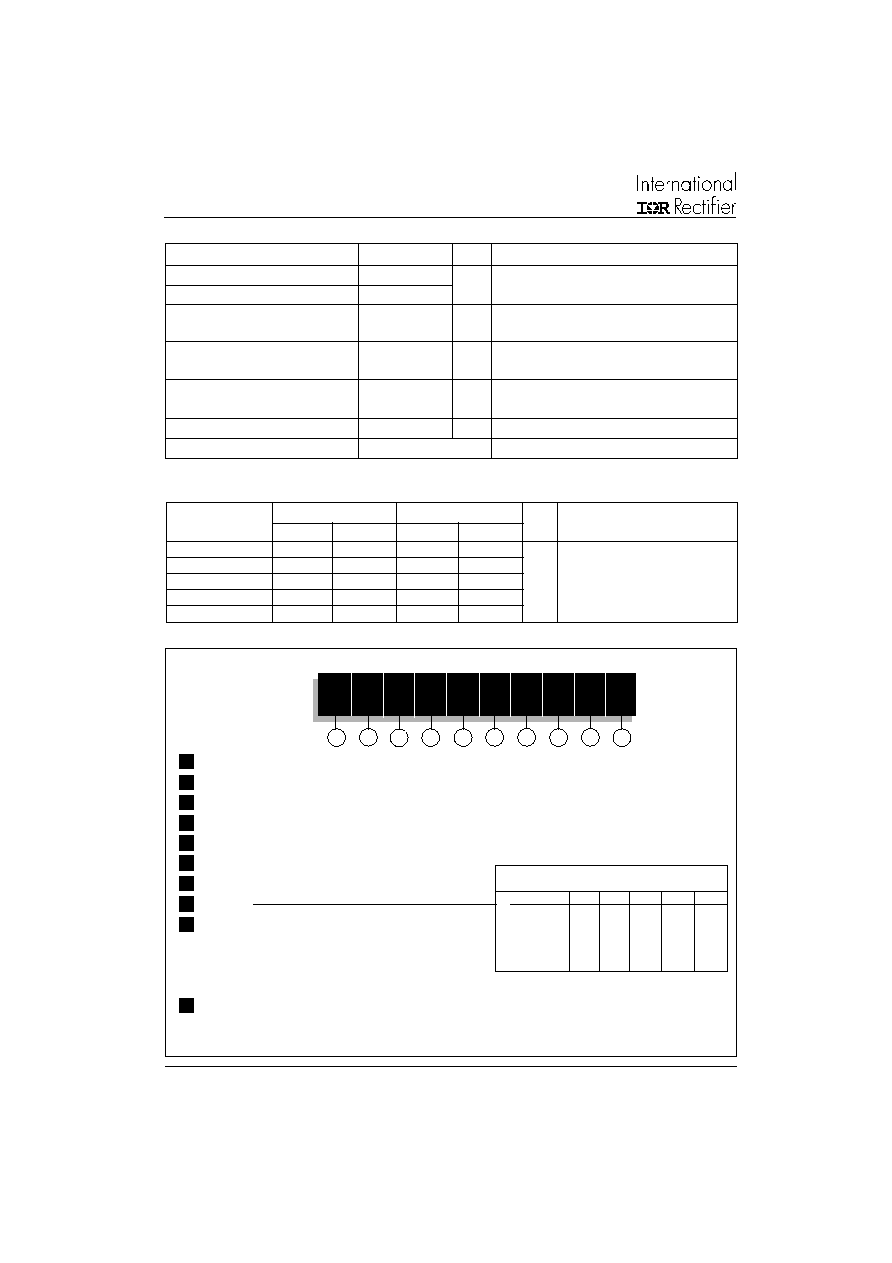
Ordering Information Table
5
6
8
9
ST
17
3
C
12
C
H
K
1
3
4
10
7
Device Code
1
2
1
- Thyristor
2
- Essential part number
3
- 3 = Fast turn off
4
- C = Ceramic Puk
5
- Voltage code: Code x 100 = V
RRM
(See Voltage Rating Table)
6
- C = Puk Case TO-200AB (A-PUK)
7
- Reapplied dv/dt code (for t
q
test condition)
8
- t
q
code
9
- 0 = Eyelet term. (Gate and Aux. Cathode Unsoldered Leads)
1 = Fast-on term. (Gate and Aux. Cathode Unsoldered Leads)
2 = Eyelet term. (Gate and Aux. Cathode Soldered Leads)
3 = Fast-on term. (Gate and Aux. Cathode Soldered Leads)
- Critical dv/dt:
None = 500V/µsec (Standard value)
L
= 1000V/µsec (Special selection)
10
t
q
(µs)
dv/dt - t
q
combinations available
dv/dt (V/µs)
20
50
100
200
400
15
CL
--
--
--
--
18
CP
DP
EP
FP *
--
20
CK
DK
EK
FK *
HK
25
CJ
DJ
EJ
FJ
HJ
30
--
DH
EH
FH
HH
*
Standard part number.
All other types available only on request.
ST173C..C Series
5
Bulletin I25180 rev. B 04/00
www.irf.com
Fig. 1 - Current Ratings Characteristics
Fig. 2 - Current Ratings Characteristics
40
50
60
70
80
90
1 0 0
1 1 0
1 2 0
1 3 0
0
4 0
80
1 2 0
16 0
2 00
24 0
30∞
60 ∞
90∞
120∞
18 0∞
Av erage On -state Current (A)
C o nd uc tio n A ng le
M
a
x
i
mu
m
A
l
l
o
w
a
bl
e
He
at
s
i
n
k
T
e
m
p
e
r
at
u
r
e
(
∞
C
)
ST173C..C Series
(Sin gle Side Cooled)
R (D C) = 0.17 K/W
th J -hs
2 0
3 0
4 0
5 0
6 0
7 0
8 0
9 0
1 0 0
1 1 0
1 2 0
1 3 0
0
5 0
1 0 0
1 5 0
2 0 0
2 5 0
3 0 0
3 5 0
D C
3 0 ∞
6 0 ∞
9 0 ∞
1 2 0 ∞
1 8 0 ∞
A v e ra g e O n -st a te C u rre n t ( A )
C o nd u ct io n Pe rio d
M
a
x
i
mu
m A
l
l
o
w
a
b
l
e
H
e
a
t
s
i
n
k
T
e
mp
e
r
a
t
u
r
e
(
∞
C)
ST 1 7 3 C ..C S e rie s
( Sin g le S id e C o o le d )
R ( D C ) = 0 .1 7 K / W
thJ -hs
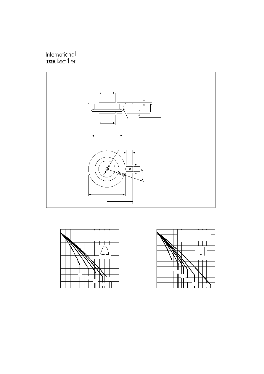
Outline Table
Case Style TO-200AB (A-PUK)
All dimensions in millimeters (inches)
DIA. MAX.
4.75 (0.19)
28 (1.10)
6.5 (0.26)
19 (0.75)
0.3 (0.01) MIN.
0.3 (0.01) MIN.
13.7 / 14.4
(0.54 / 0.57)
25∞± 5∞
GATE TERM. FOR
1.47 (0.06) DIA.
PIN RECEPTACLE
ANODE TO GATE
CREEPAGE DISTANCE: 7.62 (0.30) MIN.
STRIKE DISTANCE: 7.12 (0.28) MIN.
19 (0.75)
DIA. MAX.
38 (1.50) DIA MAX.
2 HOLES 3.56 (0.14) x
1.83 (0.07) MIN. DEEP
42 (1.65) MAX.
Quote between upper and lower
pole pieces has to be considered
after application of Mounting Force
(see Thermal and Mechanical
Specification)
ST173C..C Series
6
Bulletin I25180 rev. B 04/00
www.irf.com
Fig. 7 - Maximum Non-repetitive Surge Current
Single and Double Side Cooled
Fig. 8 - Maximum Non-repetitive Surge Current
Single and Double Side Cooled
Fig. 5 - On-state Power Loss Characteristics
Fig. 6 - On-state Power Loss Characteristics
Fig. 3 - Current Ratings Characteristics
Fig. 4 - Current Ratings Characteristics
2 0
3 0
4 0
5 0
6 0
7 0
8 0
9 0
1 0 0
1 1 0
1 2 0
1 3 0
0
1 0 0
2 0 0
3 0 0
4 0 0
5 0 0
6 0 0
7 0 0
D C
3 0 ∞
6 0 ∞
9 0 ∞
1 2 0 ∞
1 8 0 ∞
A v e ra g e O n -st a t e C urr e n t (A )
C o nd u ctio n Pe rio d
M
a
x
i
mu
m
A
l
l
o
w
a
b
l
e
H
e
a
t
s
i
n
k
T
e
mp
e
r
a
t
u
r
e
(
∞
C)
ST 1 7 3 C ..C Se rie s
( D o u b le Sid e C o o le d )
R ( D C ) = 0 .0 8 K / W
th J- hs
3 0
4 0
5 0
6 0
7 0
8 0
9 0
1 0 0
1 1 0
1 2 0
1 3 0
0
5 0
1 0 0 1 5 0 2 0 0 2 5 0 3 0 0 3 5 0 4 0 0
3 0 ∞
6 0 ∞
9 0 ∞
1 2 0 ∞
1 8 0 ∞
A v e ra g e O n - sta t e C u rre n t ( A )
C on d uc tion A ng le
M
a
x
i
m
u
m
A
l
l
o
w
a
b
l
e
H
e
a
t
s
i
n
k
T
e
m
p
er
a
t
u
r
e (
∞
C)
ST 1 7 3 C ..C S e rie s
( D o ub le Sid e C o o le d )
R ( D C ) = 0 .0 8 K/ W
thJ -h s
0
2 0 0
4 0 0
6 0 0
8 0 0
1 0 0 0
1 2 0 0
1 4 0 0
0
1 0 0
2 0 0
3 0 0
4 0 0
5 0 0
6 0 0
7 0 0
D C
1 8 0 ∞
1 2 0 ∞
9 0 ∞
6 0 ∞
3 0 ∞
R M S L im it
Co nd uc tio n Pe riod
M
a
x
i
m
u
m
A
v
er
a
g
e O
n
-
s
t
a
t
e
P
o
w
e
r
L
o
s
s
(
W
)
A v e ra g e O n -st a te C u rre n t (A )
ST 1 7 3 C ..C Se r ie s
T = 1 2 5 ∞C
J
0
1 0 0
2 0 0
3 0 0
4 0 0
5 0 0
6 0 0
7 0 0
8 0 0
9 0 0
1 0 0 0
0
5 0 1 0 0 1 5 0 2 0 0 2 5 0 3 0 0 3 5 0 4 0 0 4 5 0
1 8 0 ∞
1 2 0 ∞
9 0 ∞
6 0 ∞
3 0 ∞
R M S L im it
Co nd uctio n A ng le
M
a
x
i
mu
m A
v
e
r
a
g
e
O
n
-
s
t
a
t
e
P
o
w
e
r
L
o
s
s
(
W
)
A v e ra g e O n -st a te C u rre n t ( A )
S T 1 7 3 C ..C Se rie s
T = 1 2 5 ∞ C
J
2 0 0 0
2 5 0 0
3 0 0 0
3 5 0 0
4 0 0 0
4 5 0 0
1
1 0
1 0 0
N um b er O f E q ua l A m p litud e H a lf C yc le C urre n t Pulse s (N )
A t A n y R a te d L o a d C o n d it io n A n d W it h
R a t e d V A p p lie d F o llo w in g S u rg e .
RRM
P
e
ak
Hal
f
S
i
n
e
W
a
v
e
O
n
-
s
t
a
t
e
C
u
r
r
e
n
t
(
A
)
In it ia l T = 1 2 5 ∞ C
@ 6 0 H z 0 .0 0 8 3 s
@ 5 0 H z 0 .0 1 0 0 s
J
ST 1 7 3 C ..C S e rie s
1 5 0 0
2 0 0 0
2 5 0 0
3 0 0 0
3 5 0 0
4 0 0 0
4 5 0 0
5 0 0 0
0 .0 1
0 .1
1
P u lse T ra in D u ra tio n ( s)
V e rsu s P ulse T ra in D u ra t io n . C o n t ro l
O f C o n d u c t io n M a y N o t B e M a in t a in e d .
P
e
ak
Hal
f
S
i
n
e
W
a
v
e
O
n
-
s
t
a
t
e
C
u
r
r
e
n
t
(
A
)
In it ia l T = 1 2 5 ∞ C
N o V o lt a g e R e a p p lie d
Ra t e d V R e a p p lie d
RRM
J
ST 1 7 3 C ..C S e rie s
M a x im u m N o n R e p e t it iv e S urg e C u rre n t
ST173C..C Series
7
Bulletin I25180 rev. B 04/00
www.irf.com
Fig. 9 - On-state Voltage Drop Characteristics
Fig. 10 - Thermal Impedance Z
thJ-hs
Characteristics
Fig. 11 - Reverse Recovered Charge Characteristics
Fig. 12 - Reverse Recovery Current Characteristics
Fig. 13 - Frequency Characteristics
10 0
1 0 00
10 0 00
1
1 .5
2
2 .5
3
3.5
4
4 .5
T = 25 ∞C
I
n
st
a
n
t
a
n
e
o
u
s
O
n
-
s
t
a
t
e
C
u
rre
n
t
(
A
)
Instantan eous On -state Voltage (V)
T = 125 ∞C
J
ST1 73C ..C Series
J
0
5 0
1 0 0
1 5 0
2 0 0
2 5 0
0
20
40
6 0
8 0
1 0 0
I = 5 00 A
3 0 0 A
2 0 0 A
10 0 A
50 A
Rate O f Fall Of O n-state Current - di/dt (A/µs)
M
a
x
i
m
u
m
R
e
ve
r
s
e
R
e
c
o
ve
ry
C
h
a
r
g
e
-
Q
rr (
µ
C
)
ST173 C..C Ser ies
T = 12 5 ∞C
J
T M
0 .0 0 1
0 .0 1
0 .1
1
0 .0 0 1
0 . 0 1
0 . 1
1
1 0
S q u a re W a v e P u lse D ur at io n ( s)
th
J
-
h
s
T
r
a
n
s
i
e
n
t
T
h
e
r
m
a
l
I
m
pe
d
a
n
c
e
Z
(
K
/
W
)
S T 1 7 3 C ..C Se rie s
S t e a d y S ta t e V a lu e
R = 0 .1 7 K / W
( S in g le S id e C o o le d )
R = 0 .0 8 K / W
( D o u b le S id e C o o le d )
( D C O p e ra t io n )
th J- hs
th J- hs
1 E 2
1 E 3
1 E 4
1 E 1
1 E 2
1 E 3
1 E 4
50 H z
400
2 50 0
1 00
P u lse Ba se w id t h ( µ s)
P
e
a
k
O
n
-
s
t
a
t
e
C
u
rre
n
t
(
A
)
100 0
1 50 0
3 000
2 00
500
5 00 0
ST1 73 C.. C Serie s
Sinus o id a l p ulse
T = 40 ∞C
C
Snu b b e r c irc uit
R = 47 oh m s
C = 0.22 µF
V = 80% V
s
s
D
DR M
t p
1 E 4 1 E 1
1 E 2
1 E 3
1 E 4
50 H z
40 0
2 50 0
10 0
Pu lse B a se w id th ( µ s)
10 00
1 50 0
30 0 0
20 0
50 0
5 0 00
ST1 73C ..C Serie s
Sinus oid a l p ulse
T = 55∞C
C
Snub b er c irc uit
R = 47 o hm s
C = 0 .22 µF
V = 8 0% V
s
s
D
D R M
tp
1 E 1
0
2 0
4 0
6 0
8 0
1 0 0
1 2 0
1 4 0
1 6 0
0
2 0
4 0
6 0
8 0
1 0 0
M
a
x
i
m
u
m
R
e
v
e
rs
e
R
e
c
o
v
e
ry
C
u
rre
n
t
-
I
r
r
(
A
)
R a t e O f Fa ll O f F o rw a r d C u rre n t - d i/ d t ( A / µ s)
I = 5 00 A
30 0 A
2 00 A
1 00 A
5 0 A
S T1 73 C . . C S e rie s
T = 1 2 5 ∞C
J
TM
ST173C..C Series
8
Bulletin I25180 rev. B 04/00
www.irf.com
Fig. 16 - Maximum On-state Energy Power Loss Characteristics
Fig. 15 - Frequency Characteristics
Fig. 14 - Frequency Characteristics
1 E 1
1 E 2
1 E 3
1 E 4
1 E 1
1 E 2
1 E 3
1 E 4
50 H z
400
2 50 0
10 0
Pu lse B a se w id t h ( µ s)
P
e
a
k
O
n
-
s
ta
te
C
u
r
r
e
n
t
(
A
)
10 00
15 00
3 00 0
20 0
500
5 000
ST17 3C ..C Se ries
Tra p e zoid a l p uls e
T = 40∞C
d i/d t = 1 00 A/µs
C
Sn ub b e r c irc uit
R = 4 7 o hm s
C = 0 .22 µF
V = 8 0% V
s
s
D
D RM
tp
10 00 0
1 E 4
1 E 1
1 E 2
1 E 3
1 E 4
50 H z
40 0
2 50 0
1 00
P u lse B ase w id t h ( µ s)
1 000
1 50 0
20 0
5 00
ST1 73 C..C Serie s
Tra p ezo id a l p u ls e
T = 55∞C
d i/d t = 10 0A /µs
C
3 00 0
Snub b e r c irc uit
R = 47 o hm s
C = 0 .22 µF
V = 8 0% V
s
s
D
D RM
tp
5 0 00
10 00 0
1 E 1
1 E 1
1 E 2
1 E 3
1 E 4
50 H z
400
2 50 0
100
P ulse B a se w idt h (µ s)
10 00
1 50 0
2 00 0
2 00
5 00
ST17 3C. .C Se ries
Tra p ezo id a l p uls e
T = 5 5∞C
d i/d t = 5 0A/µs
C
Snub b er c ircuit
R = 47 o hm s
C = 0 .22 µ F
V = 8 0% V
s
s
D
D RM
tp
3 00 0
5 00 0
1 E 1
1 E 2
1 E 3
1 E 4
1 E 1
1 E 2
1 E 3
1 E 4
50 H z
4 00
2 50 0
1 00
1 00 0
1 5 00
2 00 0
30 00
2 00
50 0
Pu lse B a se w id th ( µ s)
P
e
a
k
O
n
-
s
ta
t
e
C
u
r
r
e
n
t
(
A
)
ST173 C. .C Se ries
Tra p ezo id a l p uls e
T = 40 ∞C
d i/d t = 5 0A/µs
C
Snu b b e r c irc uit
R = 47 o hm s
C = 0 .22 µF
V = 8 0% V
s
s
D
D RM
tp
5 00 0
1 E 4
1 E 1
1 E 2
1 E 3
1 E 4
P u lse Ba se w id th ( µs)
20 jo ules p e r p ulse
1
0 .5
0.3
0 .2
0 .1
ST1 73 C..C Serie s
Rec ta ngula r p ulse
d i/d t = 50 A/µs
10
5
3
tp
2
1 E 1
1 E 1
1 E 2
1 E 3
1 E 4
1 E 5
1 E 1
1 E 2
1 E 3
1 E 4
P u lse B a se w id th ( µ s)
20 jo ule s p e r p uls e
2
1
0.5
0.3
0 .2
0.1
1 0
5
P
e
a
k
O
n
-
s
ta
te
C
u
r
r
e
n
t
(
A
)
3
ST17 3C ..C Serie s
Sinuso id a l p uls e
t p
1 E 4
ST173C..C Series
9
Bulletin I25180 rev. B 04/00
www.irf.com
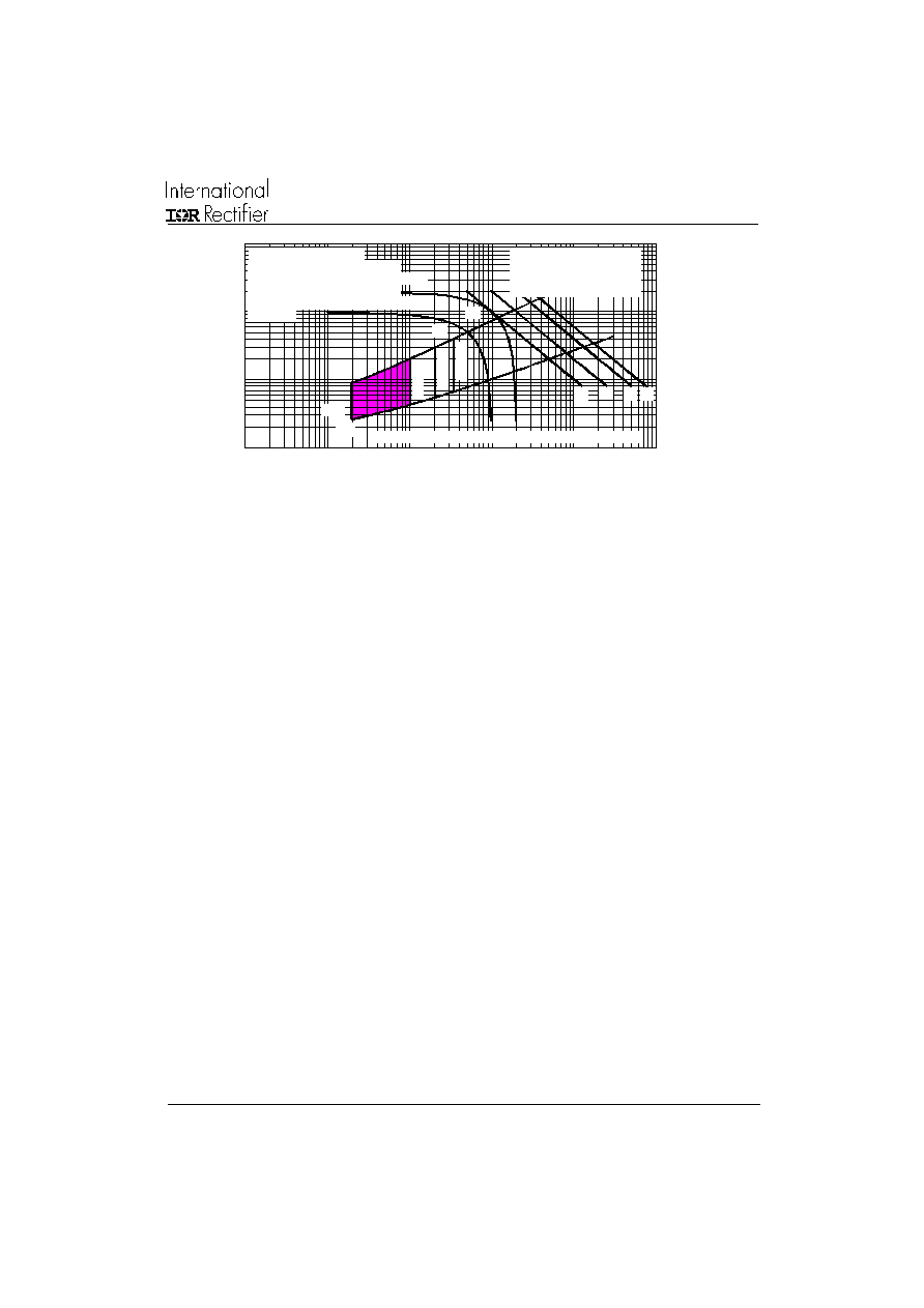
Fig. 17 - Gate Characteristics
0 . 1
1
1 0
1 0 0
0 . 0 0 1
0 . 0 1
0 . 1
1
1 0
1 0 0
V G D
IG D
( b )
(a )
Tj
=
2
5
∞
C
T
j
=
1
25
∞
C
T
j
=
-
40
∞
C
( 1 )
( 2 )
In st a n t a n e o u s G a t e C u rre n t ( A )
I
n
st
a
n
t
a
n
e
o
u
s G
a
t
e
V
o
l
t
ag
e
(
V
)
Re c ta n g ula r g a t e p ulse
a ) R e c o m m e n d e d lo a d lin e f o r
b ) R e c o m m e n d e d lo a d lin e fo r
< = 3 0 % ra t e d di/ dt : 1 0 V , 1 0 o h m s
rat e d d i/d t : 2 0 V , 1 0 o h m s; tr <= 1 µs
tr< = 1 µ s
( 1 ) PG M = 1 0 W , tp = 2 0 m s
( 2 ) PG M = 2 0 W , tp = 1 0 m s
( 3 ) PG M = 4 0 W , tp = 5 m s
( 4 ) PG M = 6 0 W , tp = 3 . 3 m s
( 3 )
D e v ic e : ST 1 7 3 C . .C S e rie s F re q u e n c y L im ite d b y PG (A V )
( 4 )