ST203S SERIES
INVERTER GRADE THYRISTORS
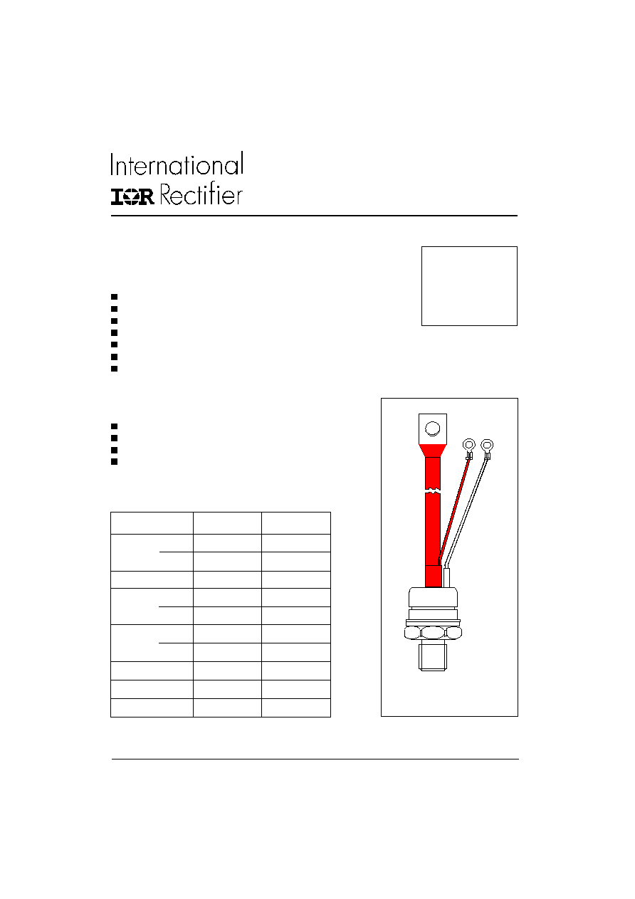
Stud Version
205A
1
Bulletin I25177 rev. C 12/96
www.irf.com
Features
All diffused design
Center amplifying gate
Guaranteed high dv/dt
Guaranteed high di/dt
High surge current capability
Low thermal impedance
High speed performance
Typical Applications
Inverters
Choppers
Induction heating
All types of force-commutated converters
I
T(AV)
205
A
@ T
C
85
∞C
I
T(RMS)
320
A
I
TSM
@
50Hz
5260
A
@ 60Hz
5510
A
I
2
t
@
50Hz
138
KA
2
s
@ 60Hz
126
KA
2
s
V
DRM
/V
RRM
1000 to 1200
V
t
q
range
20 to 30
µs
T
J
- 40 to 125
∞C
Parameters
ST203S
Units
Major Ratings and Characteristics
case style
TO-209AB (TO-93)
ST203S Series
2
Bulletin I25177 rev. C 12/96
www.irf.com
Voltage
V
DRM
/V
RRM
, maximum
V
RSM
, maximum
I
DRM
/I
RRM
max.
Type number
Code
repetitive peak voltage
non-repetitive peak voltage
@ T
J
= T
J
max.
V
V
mA
10
1000
1100
12
1200
1300
ELECTRICAL SPECIFICATIONS
Voltage Ratings
ST203S
40
Frequency
Units
50Hz
580
400
900
640
6180
4680
400Hz
570
380
940
650
2980
2150
1000Hz
520
320
930
630
1730
1200
A
2500Hz
370
210
780
510
890
580
Recovery voltage Vr
50
50
50
50
50
50
Voltage before turn-on Vd
V
DRM
V
DRM
V
DRM
Rise of on-state current di/dt
50
50
-
-
-
-
A/
µ
s
Case temperature
60
85
60
85
60
85
∞C
Equivalent values for RC circuit
47
/ 0.22µF
47
/ 0.22µF
47
/ 0.22µF
I
TM
180
o
el
180
o
el
100
µ
s
I
TM
I
TM
Current Carrying Capability
V
I
T(AV)
Max. average on-state current
205
A
180∞ conduction, half sine wave
@ Case temperature
85
∞C
I
T(RMS)
Max. RMS on-state current
320
DC @ 76∞C case temperature
I
TSM
Max. peak, one half cycle,
5260
t = 10ms
No voltage
non-repetitive surge current
5510
A
t = 8.3ms
reapplied
4420
t = 10ms
100% V
RRM
4630
t = 8.3ms
reapplied
Sinusoidal half wave,
I
2
t
Maximum I
2
t for fusing
138
t = 10ms
No voltage
Initial T
J
= T
J
max
126
t = 8.3ms
reapplied
98
t = 10ms
100% V
RRM
89
t = 8.3ms
reapplied
I
2
t
Maximum I
2
t for fusing
1380
KA
2
s
t = 0.1 to 10ms, no voltage reapplied
Parameter
ST203S
Units
Conditions
On-state Conduction
KA
2
s
ST203S Series
3
Bulletin I25177 rev. C 12/96
www.irf.com
V
TM
Max. peak on-state voltage
1.72
I
TM
= 600A, T
J
= T
J
max, t
p
= 10ms sine wave pulse
V
T(TO)1
Low level value of threshold
voltage
V
T(TO)2
High level value of threshold
voltage
r
t
1
Low level value of forward
slope resistance
r
t
2
High level value of forward
slope resistance
I
H
Maximum holding current
600
T
J
= 25∞C, I
T
> 30A
I
L
Typical latching current
1000
T
J
= 25∞C, V
A
= 12V, Ra = 6
,
I
G
= 1A
Parameter
ST203S
Units
Conditions
On-state Conduction
1.17
(16.7% x
x I
T(AV)
< I <
x I
T(AV)
), T
J
= T
J
max.
1.20
(I >
x I
T(AV)
), T
J
= T
J
max.
V
0.92
(16.7% x
x I
T(AV)
< I <
x I
T(AV)
), T
J
= T
J
max.
0.87
(I >
x I
T(AV)
), T
J
= T
J
max.
m
mA
di/dt
Max. non-repetitive rate of rise
T
J
= T
J
max, V
DRM
= rated V
DRM
of turned-on current
I
TM
= 2 x di/dt
T
J
= 25∞C, V
DM
= rated V
DRM
,
I
TM
= 50A DC, t
p
= 1µs
Resistive load, Gate pulse: 10V, 5
source
T
J
= T
J
max,
I
TM
= 300A, commutating di/dt
= 20A/µs
V
R
= 50V, t
p
= 500µs, dv/dt: see table in device code
Switching
Parameter
ST203S
Units
Conditions
1000
A/µs
t
d
Typical delay time
0.79
Min
Max
dv/dt
Maximum critical rate of rise of
T
J
= T
J
max., linear to 80% V
DRM
, higher value
off-state voltage
available on request
I
RRM
Max. peak reverse and off-state
I
DRM
leakage current
Parameter
ST203S
Units
Conditions
Blocking
500
V/
µ
s
40
mA
T
J
= T
J
max, rated V
DRM
/V
RRM
applied
P
GM
Maximum peak gate power
60
P
G(AV)
Maximum average gate power
10
I
GM
Max. peak positive gate current
10
A
T
J
= T
J
max, t
p
5ms
+V
GM
Maximum peak positive
gate voltage
-V
GM
Maximum peak negative
gate voltage
I
GT
Max. DC gate current required
to trigger
V
GT
Max. DC gate voltage required
to trigger
I
GD
Max. DC gate current not to trigger
20
mA
V
GD
Max. DC gate voltage not to trigger
0.25
V
Triggering
Parameter
ST203S
Units
Conditions
20
5
V
T
J
= T
J
max, t
p
5ms
200
mA
3
V
T
J
= 25∞C, V
A
= 12V, Ra = 6
T
J
= T
J
max, rated V
DRM
applied
µs
W
T
J
= T
J
max, f = 50Hz, d% = 50
t
q
Max. turn-off time
20
30
ST203S Series
4
Bulletin I25177 rev. C 12/96
www.irf.com
Ordering Information Table
T
J
Max. junction operating temperature range
-40 to 125
T
stg
Max. storage temperature range
-40 to 150
R
thJC
Max. thermal resistance, junction to case
0.105
DC operation
R
thCS
Max. thermal resistance, case to heatsink
0.04
Mounting surface, smooth, flat and greased
T
Mounting torque, ± 10%
31
Nm
(275)
(Ibf-in)
24.5
Nm
(210)
(Ibf-in)
wt
Approximate weight
280
g
Case style
TO-209AB (TO-93)
See Outline Table
Parameter
ST203S
Units
Conditions
Thermal and Mechanical Specifications
∞C
K/W
Non lubricated threads
180∞
0.016
0.012
120∞
0.019
0.020
90∞
0.025
0.027
K/W
T
J
= T
J
max.
60∞
0.036
0.037
30∞
0.060
0.060
Conduction angle
Sinusoidal conduction
Rectangular conduction Units
Conditions
5
6
8
9
ST
20
3
S
12
P
F
J
0
3
4
10
7
Device Code
1
2
Lubricated threads
1
- Thyristor
2
- Essential part number
3
- 3 = Fast turn off
4
- S = Compression bonding Stud
5
- Voltage code: Code x 100 = V
RRM
(See Voltage Ratings table)
6
- P = Stud base 3/4" 16UNF-2A
M = Stud base metric threads M16/ x 1.5
7
- Reapplied dv/dt code (for t
q
test condition)
8
- t
q
code
9
- 0 = Eyelet terminals (Gate and Aux. Cathode Leads)
1 = Fast-on terminals (Gate and Aux. Cathode Leads)
2 = Flag terminals (For Cathode and Gate Terminals)
- Critical dv/dt:
None = 500V/µsec (Standard value)
L
= 1000V/µsec (Special selection)
dv/dt - t
q
combinations available
dv/dt (V/µs)
20
50
100
200
400
20
CK
DK
EK
--
--
25
CJ
DJ
EJ
FJ *
--
30
CH
DH
EH
FH
HH
t
q
(µs)
R
thJC
Conduction
(The following table shows the increment of thermal resistence R
thJC
when devices operate at different conduction angles than DC)
*
Standard part number.
All other types available only on request.
10
ST203S Series
5
Bulletin I25177 rev. C 12/96
www.irf.com
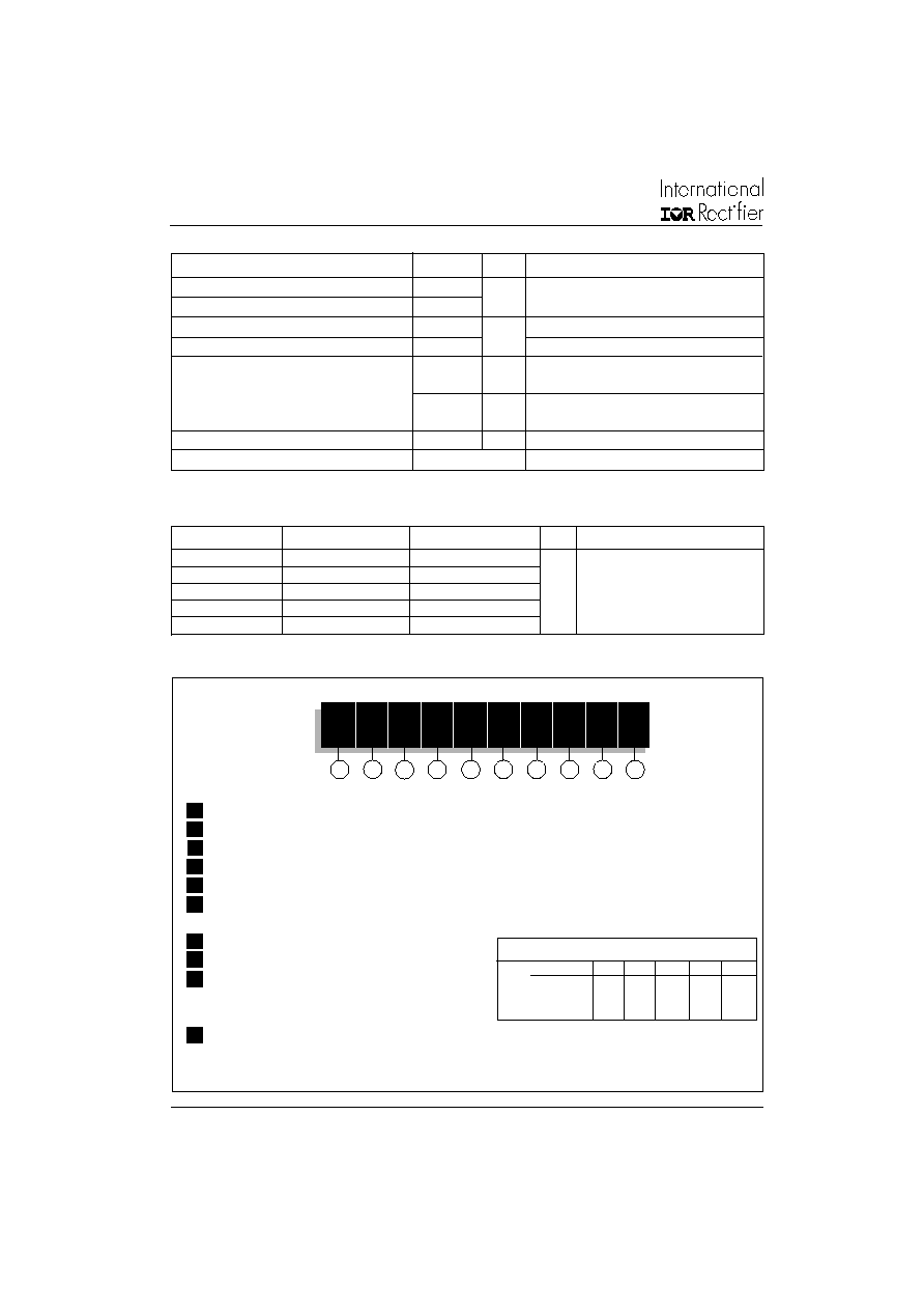
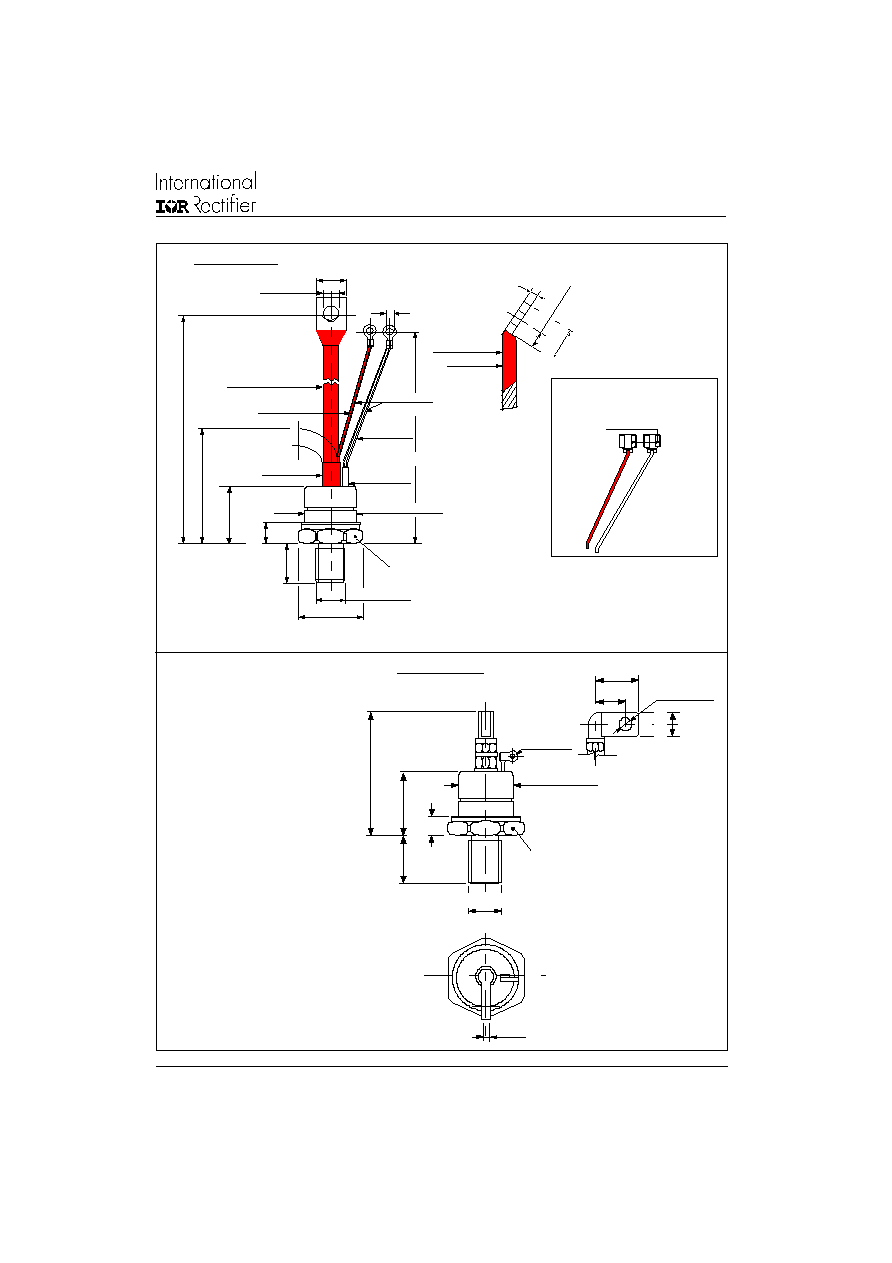
Case Style TO-209AB (TO-93)
All dimensions in millimeters (inches)
Fast-on Terminals
Outline Table
Case Style TO-209AB (TO-93) Flag
All dimensions in millimeters (inches)
CERAMIC HOUSING
27
.
5
(1
.
08)
M
A
X.
3
8
.
5
(
1
.5
2
)
MA
X
.
3 (0.12)
80
(
3
.
15) M
A
X.
DIA. 27.5 (1.08) MAX.
16
(0
.
63) M
A
X.
FLAG TERMINALS
1.5 (0.06) DIA.
SW 32
22 (0.89)
DIA. 6.5 (0.25)
13 (0.
5
1)
14 (0.55)
*FOR METRIC DEVICE. M16 X 1.5 - LENGHT 21 (0.83) MAX.
3/4"-16UNF-2A*
AMP. 280000-1
REF-250
2
WHITE SHRINK
RED SHRINK
RED CATHODE
RED SILICON RUBBER
+I
210 (
8
.
26)
10 (
0
.
39)
C.S. 0.4mm
(0.0006 s.i.)
38.
5 (
1
.
52)
MA
X
.
+-
220 (8.66) 10 (0.39)
CERAMIC HOUSING
90 (
3
.
54)
M
I
N
.
4.3 (0.17) DIA.
19 (0.75) MAX.
8.5 (0.33) DIA.
* FOR METRIC DEVICE : M16 x 1.5 - LENGHT 21 (0.83) MAX.
C.S. 25mm 2
(0.039 s.i.)
FLEXIBLE LEAD
4 (0.16) MAX.
2
2
(
0
.8
6
)
MI
N
.
MA
X
.
35 (1.38) MAX.
3/4"-16UNF-2A *
27.
5 (
1
.
08)
SW 32
27.5 (1.08) MAX. DIA.
WHITE GATE
9
.5
(
0
.3
7
)
MI
N
.
16
(
0
.
63)
M
A
X
.
ST203S Series
6
Bulletin I25177 rev. C 12/96
www.irf.com
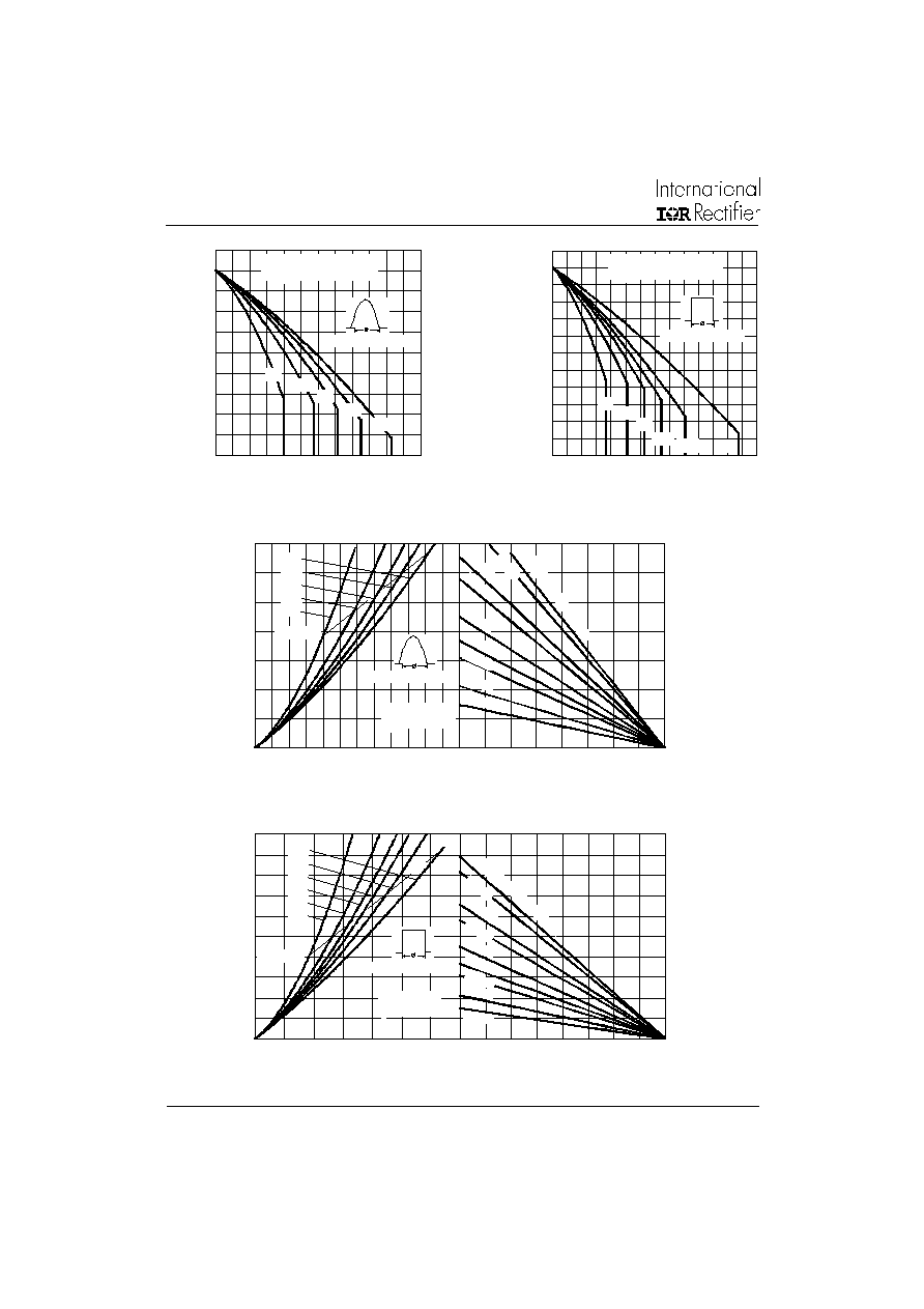
Fig. 3 - On-state Power Loss Characteristics
Fig. 1 - Current Ratings Characteristics
Fig. 2 - Current Ratings Characteristics
Fig. 4 - On-state Power Loss Characteristics
70
80
90
100
110
120
130
0
50
100
150
200
250
300
350
DC
30∞
60∞
90∞
120∞
180∞
Average On-state Current (A)
M
a
x
i
m
u
m
A
l
l
o
w
a
b
l
e
C
a
s
e
Tem
p
er
a
t
u
r
e (
∞C
)
Conduction Period
ST203S Series
R (DC) = 0.105 K/W
thJC
80
90
100
110
120
130
0
40
80
120
160
200
240
M
a
x
i
m
u
m
A
l
lo
w
a
b
l
e
C
a
s
e
T
e
m
p
er
a
t
u
r
e
(
∞C
)
30∞
60∞
90∞
120∞
180∞
Average On-state Current (A)
Conduction Angle
ST203S Series
R (DC) = 0.105 K/W
thJC
25
50
75
100
125
Maximum Allowable Ambient Temperature (∞C)
R
=
0
.0
8
K
/W
-
D
e
lta
R
th
SA
0.
1 K
/W
0.1
6 K/
W
0.2
K/
W
0.3
K/
W
0.4
K/W
0. 5
K/W
0.8 K
/W
1.2 K/W
0
50
100
150
200
250
300
350
0
40
80
120
160
200
240
180∞
120∞
90∞
60∞
30∞
RMS Limit
Conduction Angle
M
a
x
i
mu
m A
v
e
r
a
g
e
O
n
-
s
t
a
te
P
o
w
e
r
L
o
s
s
(
W
)
Average On-state Current (A)
ST203S Series
T = 125∞C
J
25
50
75
100
125
Maximum Allowable Ambient Temperature (∞C)
R
=
0
.0
8 K
/W
- D
elt
a
R
th
SA
0.1
K/
W
0.1
6 K
/W
0.2
K/W
0.3
K/W
0.4 K
/W
0.5 K
/W
0.8 K/W
1.2 K/W
0
50
100
150
200
250
300
350
400
450
500
0
50
100
150
200
250
300
350
DC
180∞
120∞
90∞
60∞
30∞
RMS Limit
Conduction Period
M
a
x
i
m
u
m
A
v
er
a
g
e
On
-
s
t
a
t
e
P
o
w
e
r
L
o
s
s
(
W
)
Average On-state Current (A)
ST203S Series
T = 125∞C
J
ST203S Series
7
Bulletin I25177 rev. C 12/96
www.irf.com
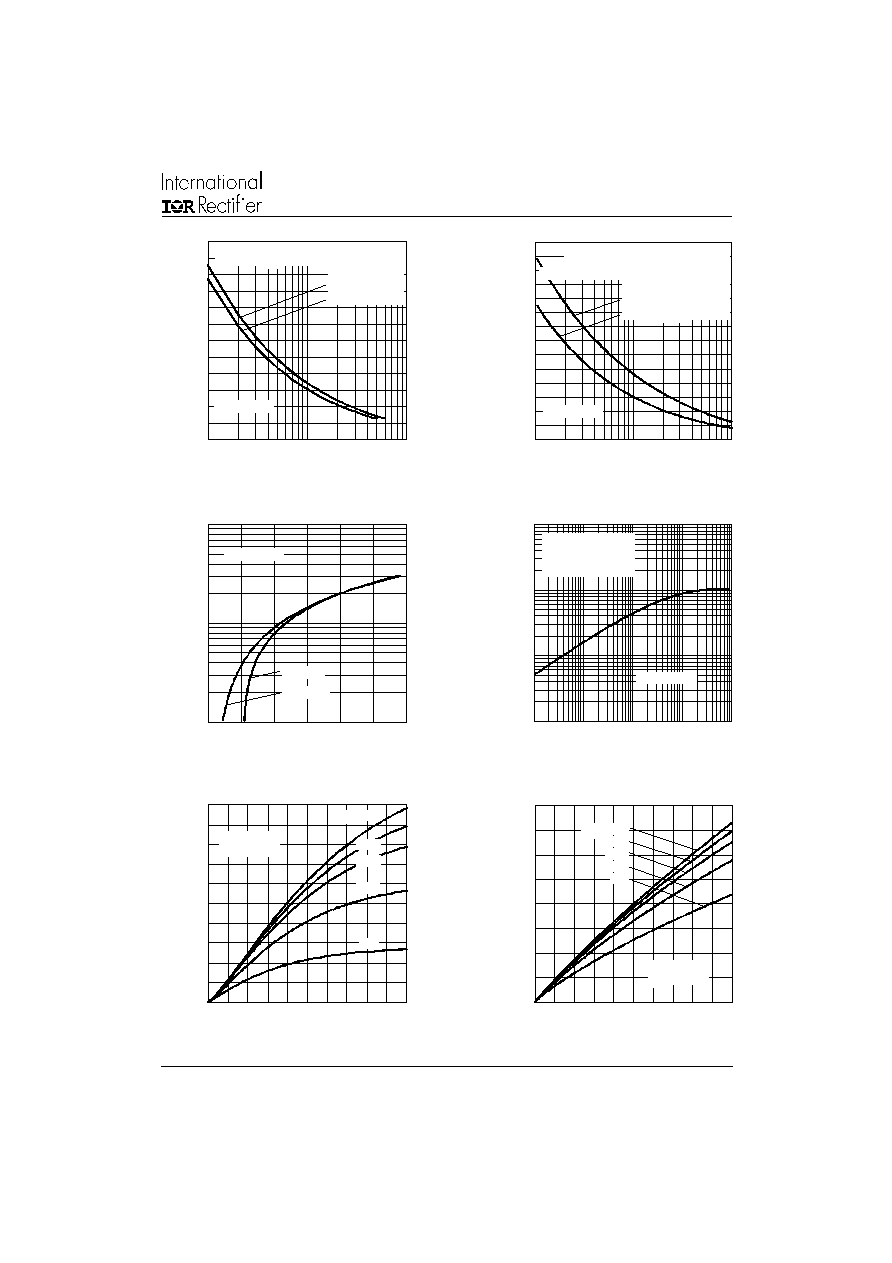
Fig. 7 - On-state Voltage Drop Characteristics
Fig. 8 - Thermal Impedance Z
thJC
Characteristic
Fig. 10 - Reverse Recovery Current Characteristics
Fig. 9 - Reverse Recovered Charge Characteristics
Fig. 5 - Maximum Non-repetitive Surge Current
Fig. 6 - Maximum Non-repetitive Surge Current
0
20
40
60
80
100
120
140
160
0
20
40
60
80
100
Rate Of Fall Of On-state Current - di/dt (A/µs)
I = 500 A
300 A
200 A
100 A
50 A
M
a
x
i
m
u
m
R
e
v
e
rs
e
R
e
c
o
v
e
ry
C
u
rre
n
t
-
Ir
r
(
A
)
ST 203S Series
T = 125 ∞C
J
TM
100
1000
10000
1
1.5
2
2.5
3
3.5
4
T = 25∞C
J
I
n
st
an
t
a
ne
o
u
s O
n
-
s
t
a
t
e
C
u
r
r
e
n
t
(
A
)
Instantaneous On-state Voltage (V)
T = 125∞C
J
ST203S Series
0
50
100
150
200
250
0
20
40
60
80
100
Rate Of Fall Of On-state Current - di/dt (A/µs)
I = 500 A
300 A
200 A
100 A
50 A
M
a
x
i
m
u
m
R
e
v
e
rs
e
R
e
c
o
v
e
ry
C
h
a
r
ge
-
Q
rr (
µC
)
ST203S Series
T = 125 ∞C
J
TM
0.001
0.01
0.1
1
0.001
0.01
0.1
1
10
Square Wave Pulse Duration (s)
th
J
C
Tr
a
n
s
i
en
t
Th
er
m
a
l
I
m
p
e
d
a
n
c
e
Z
(
K
/
W
)
Steady State Value
R = 0.105 K/W
(DC Operation)
thJC
ST203S Series
2000
2500
3000
3500
4000
4500
5000
5500
0.01
0.1
1
Pulse Train Duration (s)
Maximum Non Repetitive Surge Current
Versus Pulse Train Duration. Control
Of Conduction May Not Be Maintained.
P
e
ak
Hal
f
S
i
ne
W
a
v
e
O
n
-
s
t
a
t
e
C
u
rre
nt
(
A
)
Initial T = 125∞C
No Voltage Reapplied
Rated V Reapplied
RRM
J
ST203S Series
2000
2500
3000
3500
4000
4500
5000
1
10
100
Number Of Equal Amplitude Half Cycle Current Pulses (N)
P
e
ak
Hal
f
S
i
ne
W
a
v
e
O
n
-
s
t
a
t
e
C
u
r
r
e
n
t
(
A
)
Initial T = 125∞C
@ 60 Hz 0.0083 s
@ 50 Hz 0.0100 s
J
ST203S Series
At Any Rated Load Condition And With
Rated V Applied Following Surge.
RRM

ST203S Series
8
Bulletin I25177 rev. C 12/96
www.irf.com
Fig. 13 - Frequency Characteristics
Fig. 11 - Frequency Characteristics
Fig. 12 - Frequency Characteristics
1E1
1E2
1E3
1E4
50 Hz
400
2500
100
Pulse Basewidth (µs)
1000
1500
3000
200
500
Snubber circuit
R = 47 ohms
C = 0.22 µF
V = 80% V
s
s
D
DRM
5000
ST203S Series
Sinusoidal pulse
T = 85∞C
C
tp
1E1
1E2
1E3
1E4
1E1
1E2
1E3
1E4
50 Hz
400
2500
100
Pulse Basewidth (µs)
P
e
a
k
O
n
-
s
ta
te
C
u
r
r
e
n
t
(
A
)
1000
1500
3000
200
500
Snubber circuit
R = 47 ohms
C = 0.22 µF
V = 80% V
s
s
D
DRM
5000
ST203S Series
Sinusoidal pulse
T = 60∞C
C
1E4
tp
1E2
1E3
1E4
1E1
1E2
1E3
1E4
50 Hz
400
2500
100
1000
1500
200
Pulse Basewidth (µs)
P
e
a
k
O
n
-
s
ta
te
C
u
r
r
e
n
t
(
A
)
Snubber circuit
R = 47 ohms
C = 0.22 µF
V = 80% V
s
s
D
DRM
3000
ST203S Series
Trapezoidal pulse
T = 60∞C
di/dt = 100A/µs
C
tp
1E4
500
1E2
1E3
1E4
1E1
1E2
1E3
1E4
50 Hz
400
100
1000
1500
200
Pulse Basewidth (µs)
P
e
a
k
O
n
-
s
ta
te
C
u
r
r
e
n
t
(
A
)
5000
2500
Snubber circuit
R = 47 ohms
C = 0.22 µF
V = 80% V
s
s
D
DRM
ST203S Series
Trapezoidal pulse
T = 60∞C
di/dt = 50A/µs
C
1E4
500
3000
1E1
1E2
1E3
1E4
50 Hz
400
2500
100
1000
1500
200
Pulse Basewidth (µs)
Snubber circuit
R = 47 ohms
C = 0.22 µF
V = 80% V
s
s
D
DRM
ST203S Series
Trapezoidal pulse
T = 85∞C
di/dt = 100A/µs
C
3000
tp
500
1E1
1E1
1E2
1E3
1E4
50 Hz
400
100
1000
1500
200
Pulse Basewidth (µs)
5000
2500
Snubber circuit
R = 47 ohms
C = 0.22 µF
V = 80% V
s
s
D
DRM
ST203S Series
Trapezoidal pulse
T = 85∞C
di/dt = 50A/µs
C
500
3000
1E1
ST203S Series
9
Bulletin I25177 rev. C 12/96
www.irf.com
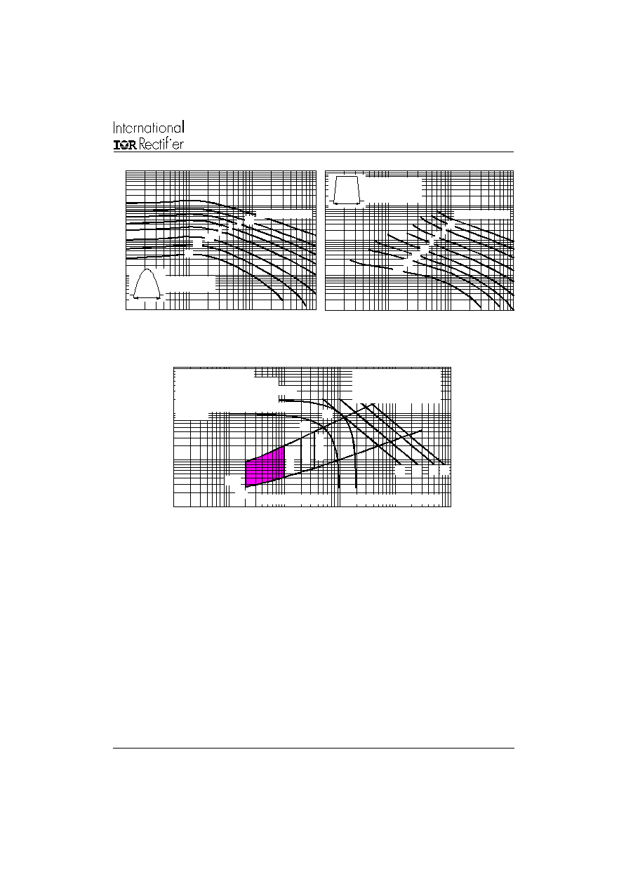
Fig. 14 - Maximum On-state Energy Power Loss Characteristics
Fig. 15 - Gate Characteristics
0.1
1
10
100
0.001
0.01
0.1
1
10
100
VGD
IGD
(b)
(a)
Tj
=
2
5
∞C
Tj
=
1
2
5
∞
C
Tj
=
-
4
0
∞
C
(1)
(2)
Instantaneous Gate Current (A)
I
n
st
a
n
t
a
n
e
o
u
s G
a
t
e
V
o
l
t
a
g
e
(
V
)
Rectangular gate pulse
a) Recommended load line for
b) Recommended load line for
<=30% rated di/dt : 10V, 10ohms
rated di/dt : 20V, 10ohms; tr<=1 µs
tr<=1 µs
(1) PGM = 10W, tp = 20ms
(2) PGM = 20W, tp = 10ms
(3) PGM = 40W, tp = 5ms
(4) PGM = 60W, tp = 3.3ms
(3)
Device: ST203S Series
(4)
Frequency Limited by PG(AV)
1E1
1E2
1E3
1E4
1E5
1E1
1E2
1E3
1E4
Pulse Basewidth (µs)
20 joules per pulse
2
1
0.2
0.1
P
e
a
k
O
n
-
s
t
a
t
e
C
u
rre
n
t
(
A
)
7.5
4
0.4
ST203S Series
Sinusoidal pulse
tp
1E4
1E1
1E2
1E3
1E4
Pulse Basewidth (µs)
20 joules per pulse
2
1
0.5
0.2
0.1
10
5
ST203S Series
Rectangular pulse
di/dt = 50A/µs
tp
1E1
0.3