 | –≠–ª–µ–∫—Ç—Ä–æ–Ω–Ω—ã–π –∫–æ–º–ø–æ–Ω–µ–Ω—Ç: ST2100C | –°–∫–∞—á–∞—Ç—å:  PDF PDF  ZIP ZIP |
2090A
PHASE CONTROL THYRISTORS
Hockey Puk Version
ST2100C..R SERIES
D-413
Bulletin I25198/A
Features
Double side cooling
High surge capability
High mean current
Fatigue free
Typical Applications
DC motor controls
Controlled DC power supplies
AC controllers
I
T(AV)
1770
A
@ T
C
80
∞C
I
T(AV)
2090
A
@ T
hs
55
∞C
I
T(RMS)
3850
A
@ T
hs
25
∞C
I
TSM
@
50Hz
36250
A
@
60Hz
38000
A
I
2
t
@
50Hz
6570
KA
2
s
@
60Hz
5990
KA
2
s
V
DRM
/V
RRM
3000 to 4200
V
t
q
typical
500
µs
T
J
max.
125
∞C
Parameters
ST2100C..R
Units
Major Ratings and Characteristics
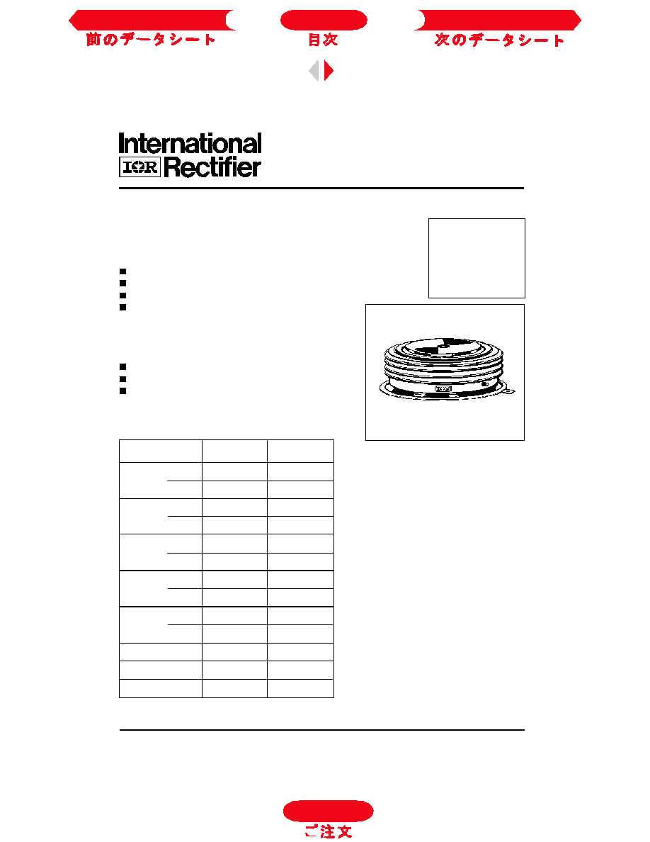
(R-PUK)
Next Data Sheet
Index
Previous Datasheet
To Order
ST2100C..R Series
2222222222222
12
D-414
Voltage
V
DRM
/V
RRM
, max. repetitive
V
RSM
, maximum non-
I
DRM
/I
RRM
max.
Type number
Code
peak and off-state voltage
repetitive peak voltage
@ T
C
= 125∞C
V
V
mA
30
3000
3100
32
3200
3300
34
3400
3500
36
3600
3700
38
3800
3900
40
4000
4100
42
4200
4300
ELECTRICAL SPECIFICATIONS
Voltage Ratings
I
T(AV)
Max. average on-state current
1770 (1150)
A
@ Case temperature
80
∞C
I
T(AV)
Max. average on-state current
2090 (940)
A
@ Heatsink temperature
55 (85)
∞C
I
T(RMS)
Max. RMS on-state current
3850
A
DC @ 25∞C heatsink temperature double side cooled
I
TSM
Max. peak, one-cycle
No voltage
non-repetitive surge current
reapplied
50% V
RRM
reapplied
Sinusoidal half wave,
I
2
t
Maximum I
2
t for fusing
No voltage
Initial T
C
= 125∞C
reapplied
50% V
RRM
reapplied
V
T(TO)
Max. value of threshold voltage
1.03
V
T
J
= T
J
max.
r
t
Max. value of on-state slope
resistance
V
TM
Max. on-state voltage
1.875
V
I
pk
= 2900A, T
C
= 25∞C
I
L
Typical latching current
300
mA
T
J
= 25∞C, V
D
=
5V
Parameter
ST2100C..R
Units
Conditions
On-state Conduction
A
KA
2
s
0.32
T
J
= T
J
max.
m
180∞ conduction, half sine wave
double side (single side [anode side]) cooled
t = 10ms
t = 8.3ms
t = 10ms
t = 8.3ms
t = 10ms
t = 8.3ms
t = 10ms
t = 8.3ms
36250
38000
29000
30350
6570
5990
4205
3820
Parameter
ST2100C..R
Units Conditions
150 (300)
A/µs
µs
t
q
Typical turn-off time
500
di/dt
Max. repetitive 50Hz (no repetitive)
From 67% V
DRM
to 1000A gate drive 20V, 10
, t
r
=
0.5µs
rate of rise of turned-on current
T
J
= T
J
max.
Gate drive 30V, 15
,
V
d
= 67% V
DRM
,
T
J
= 25∞C
Rise time 0.5µs
I
T
= 1000A, t
p
= 1ms, T
J
= T
J
max, V
RM
= 50V,
dI
RR
/dt = 2A/µs, V
DR
=
67% V
DRM
,
dV
DR
/dt
= 8V/µs linear
Switching
t
d
Maximum delay time
2.5
ST2100C..R
250
Next Data Sheet
Index
Previous Datasheet
To Order
ST2100C..R Series
D-417
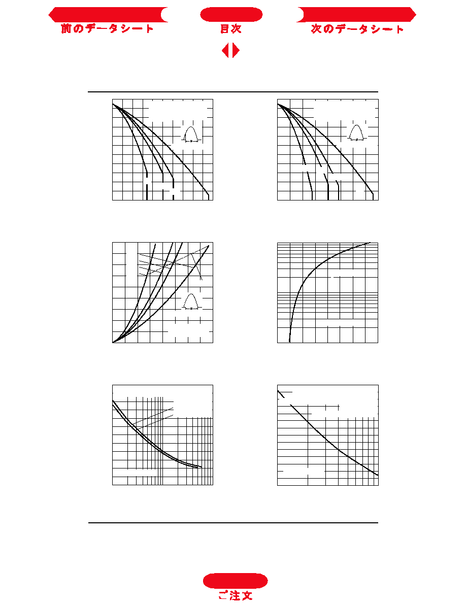
Fig. 1 - Current Ratings Characteristics
Fig. 2 - Current Ratings Characteristics
Fig. 5 - Maximum Non-Repetitive Surge Current
Fig. 6 - Maximum Non-Repetitive Surge Current
Fig. 4 - On-state Voltage Drop Characteristics
Fig. 3 - On-state Power Loss Characteristics
To Order
Next Data Sheet
Index
Previous Datasheet
ST2100C..R Series
D-418
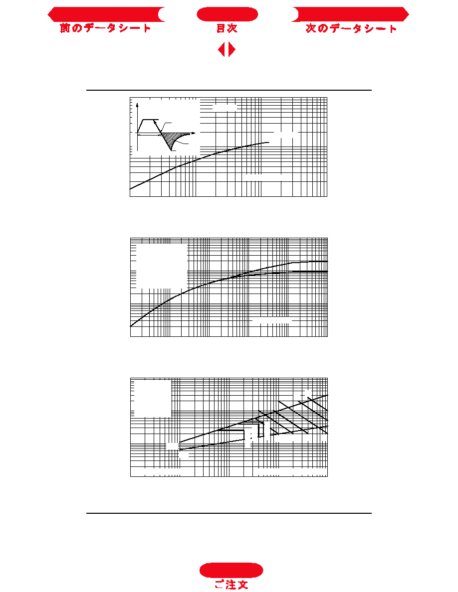
Fig. 7 - Stored Charged
Fig. 8 - Thermal Impedance Z
thJ-C
Characteristics
Fig. 9 - Gate Characteristics
To Order
Next Data Sheet
Index
Previous Datasheet
ST2100C..R Series
23
D-415
3333
dv/dt
Maximum linear rate of rise of
off-state voltage
I
RRM
Max. peak reverse and off-state
I
DRM
leakage current
500
V/µs
T
J
= T
J
max. to 67% rated V
DRM
Parameter
ST2100C..R
Units
Conditions
250
mA
T
J
= 125∞C rated V
DRM
/V
RRM
applied
Blocking
P
GM
Maximum peak gate power
150
t
p
= 100µs
P
G(AV)
Maximum average gate power
10
I
GM
Max. peak positive gate current
30
A
Anode positive with respect to cathode
V
GM
Max. peak positive gate voltage
30
V
Anode positive with respect to cathode
-V
GM
Max. peak negative gate voltage
0.25
V
Anode positive with respect to cathode
I
GT
Maximum DC gate current
required to trigger
V
GT
Maximum gate voltage required
to trigger
Parameter
ST2100C..R
Units
Conditions
W
400
mA
T
C
= 25∞C, V
DRM
= 5V
4
V
T
C
= 25∞C, V
DRM
= 5V
V
GD
DC gate voltage not to trigger
0.25
V
T
C
= 125∞C
Max. gate current/voltage not to
trigger is the max. value which
will not trigger any unit with rated
V
DRM
anode-to-cathode applied
Triggering
T
J
max. Max. operating temperature
125
On-state (conducting)
T
stg
Max. storage temperature range
-55 to 125
R
thJ-C
Thermal resistance, junction
0.019
DC operation single side cooled
to case
0.0095
DC operation double side cooled
R
th(C-h)
Thermal resistance, case
0.004
Single side cooled
to heatsink
0.002
Double side cooled
F
Mounting force ± 10%
wt
Approximate weight
1600
g
Case style
(R-PUK)
See Outline Table
Parameter
ST2100C..R
Units
Conditions
Thermal and Mechanical Specification
∞C
Clamping force 43KN with
mounting compound
43000
(4400)
N
(Kg)
R
thJ-C
Conduction
(The following table shows the increment of thermal resistence R
thJ-C
when devices operate at different conduction angles than DC)
K/W
K/W
180∞
0.0010
0.0010
T
J
= T
J
max.
120∞
0.0017
0.0017
K/W
60∞
0.0044
0.0044
Conduction angle
Single side
Double side
Units
Conditions
To Order
Next Data Sheet
Index
Previous Datasheet

ST2100C..R Series
2222222222222
12
D-416
Ordering Information Table
Device Code
5
1
2
3
4
ST
210
0
C
42
R
1
7
6
8
1
-
Thyristor
2
-
Essential part number
3
-
0 = Converter grade
4
-
C = Ceramic Puk
5
-
Voltage code: Code x 100 = V
RRM
(See Voltage Rating Table)
6
-
R = Puk Case
7
-
0 = Eyelet terminals (Gate and Auxiliary Cathode Unsoldered Leads)
1 = Fast-on terminals (Gate and Auxiliary Cathode Unsoldered Leads)
2 = Eyelet terminals (Gate and Auxiliary Cathode Soldered Leads)
3 = Fast-on terminals (Gate and Auxiliary Cathode Soldered Leads)
8
-
Critical dv/dt: None = 500V/µsec (Standard selection)
L
= 1000V/µsec (Special selection)
Outline Table
(R-PUK)
All dimensions in millimeters (inches)
112.5 (4.4) DIA. MAX.
73.2 (2.9) DIA. MAX.
TWO PLACES
GATE
1.5 (0.06) DIA.
3
7
.
7
(
1
.
5
)
M
A
X
.
ANODE
3.7 (0.15) DIA. NOM. X
2.1 (0.1) DEEP MIN.
BOTH ENDS
CATHODE
HOLE 1.5 (0.06)
DIA. MAX.
4.76 (0.2)
20∞ ± 5∞
6 .3
(0
.2
4 )
To Order
Next Data Sheet
Index
Previous Datasheet