D-480
DISCRETE POWER DIODES and THYRISTORS
DATA BOOK
Next Data Sheet
Index
Previous Datasheet
To Order
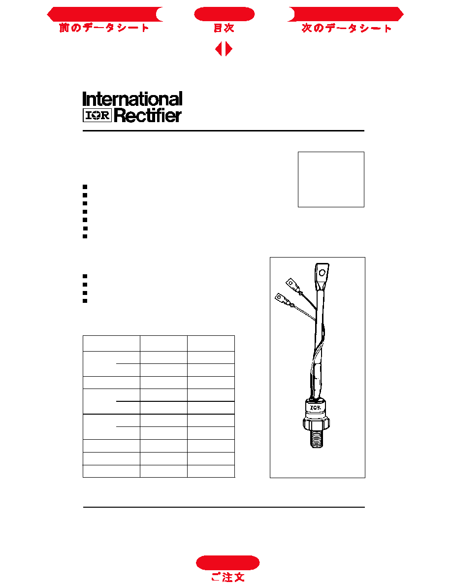
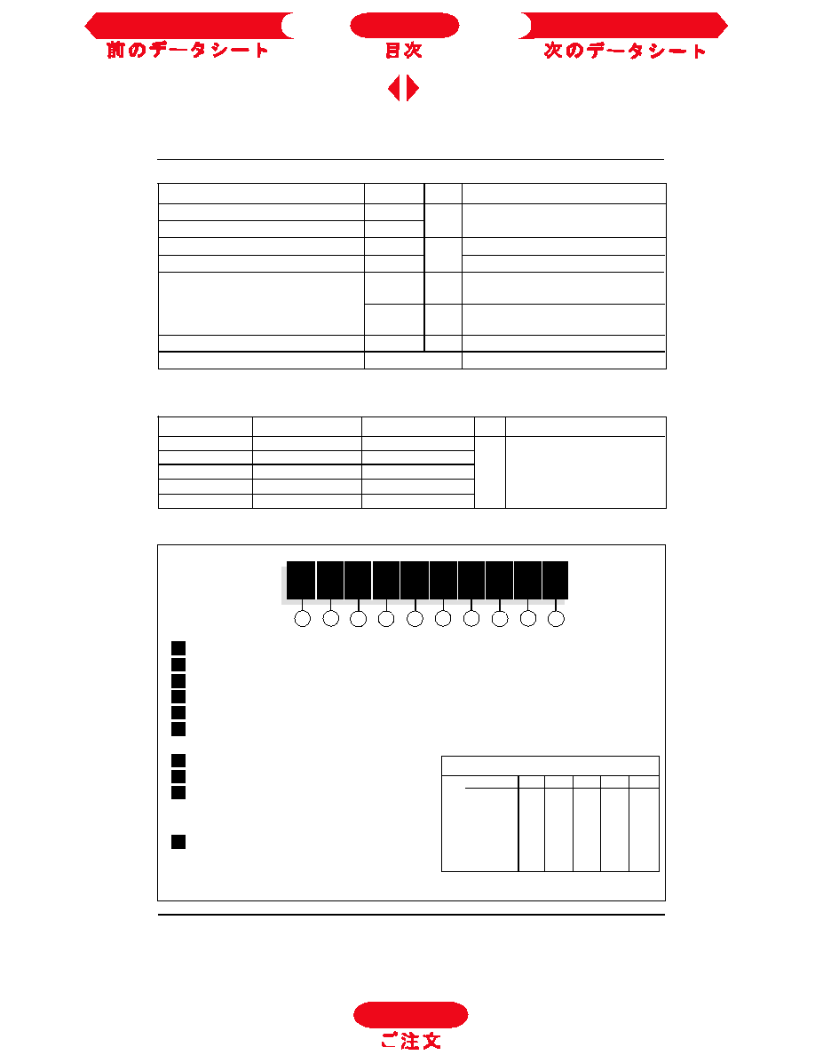
ST223S SERIES
INVERTER GRADE THYRISTORS
Stud Version
220A
D-481
Bulletin I25175/B
Features
All diffused design
Center amplifying gate
Guaranteed high dv/dt
Guaranteed high di/dt
High surge current capability
Low thermal impedance
High speed performance
Typical Applications
Inverters
Choppers
Induction heating
All types of force-commutated converters
I
T(AV)
220
A
@ T
C
85
�C
I
T(RMS)
345
A
I
TSM
@
50Hz
5850
A
@ 60Hz
6120
A
I
2
t
@
50Hz
171
KA
2
s
@ 60Hz
156
KA
2
s
V
DRM
/V
RRM
400 to 800
V
t
q
range
10 to 20
�s
T
J
- 40 to 125
�C
Parameters
ST223S
Units
Major Ratings and Characteristics
case style
TO-209AB (TO-93)
Next Data Sheet
Index
Previous Datasheet
To Order
ST223S Series
D-482
Voltage
V
DRM
/V
RRM
, maximum
V
RSM
, maximum
I
DRM
/I
RRM
max.
Type number
Code
repetitive peak voltage
non-repetitive peak voltage
@ T
J
= T
J
max.
V
V
mA
04
400
500
08
800
900
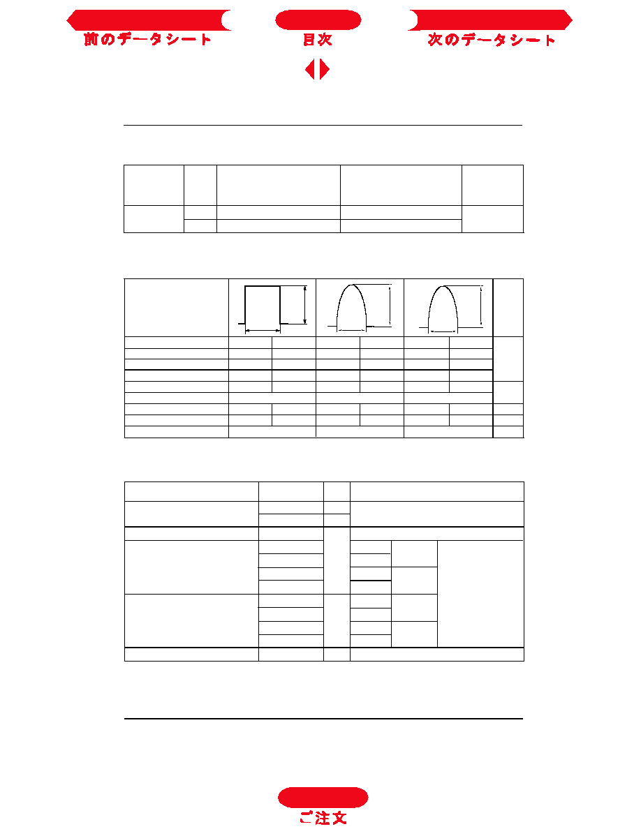
ELECTRICAL SPECIFICATIONS
Voltage Ratings
Frequency
Units
50Hz
630
430
970
690
6450
4850
400Hz
630
420
1010
710
3140
2280
1000Hz
580
370
1000
680
1860
1310
A
2500Hz
420
250
860
630
980
790
Recovery voltage Vr
50
50
50
50
50
50
Voltage before turn-on Vd
V
DRM
V
DRM
V
DRM
Rise of on-state current di/dt
50
50
-
-
-
-
A/
�
s
Case temperature
60
85
60
85
60
85
�C
Equivalent values for RC circuit
47
/ 0.22�F
47
/ 0.22�F
47
/ 0.22�F
I
TM
180
o
el
180
o
el
100
�
s
I
TM
I
TM
Current Carrying Capability
V
I
T(AV)
Max. average on-state current
220
A
180� conduction, half sine wave
@ Case temperature
85
�C
I
T(RMS)
Max. RMS on-state current
345
DC @ 76�C case temperature
I
TSM
Max. peak, one half cycle,
5850
t = 10ms
No voltage
non-repetitive surge current
6120
A
t = 8.3ms
reapplied
4920
t = 10ms
100% V
RRM
5150
t = 8.3ms
reapplied
Sinusoidal half wave,
I
2
t
Maximum I
2
t for fusing
171
t = 10ms
No voltage
Initial T
J
= T
J
max
156
t = 8.3ms
reapplied
121
t = 10ms
100% V
RRM
111
t = 8.3ms
reapplied
I
2
t
Maximum I
2
t for fusing
1710
KA
2
s
t = 0.1 to 10ms, no voltage reapplied
Parameter
ST223S
Units
Conditions
On-state Conduction
KA
2
s
ST223S
40
To Order
Next Data Sheet
Index
Previous Datasheet
ST223S Series
D-486
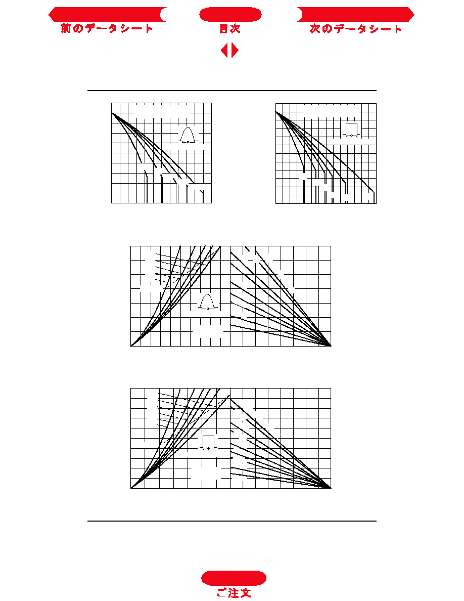
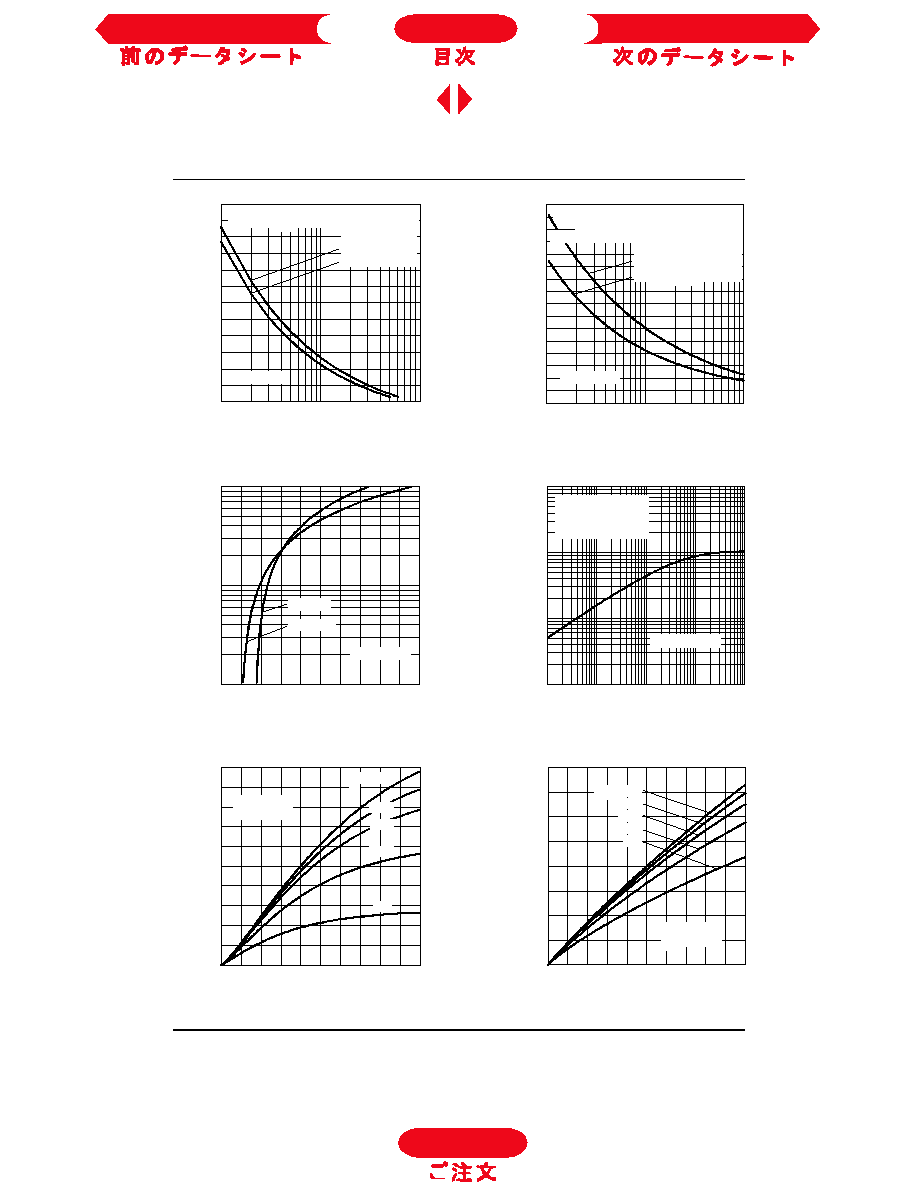
Fig. 3 - On-state Power Loss Characteristics
Fig. 1 - Current Ratings Characteristics
Fig. 2 - Current Ratings Characteristics
Fig. 4 - On-state Power Loss Characteristics
To Order
Next Data Sheet
Index
Previous Datasheet
ST223S Series
D-487
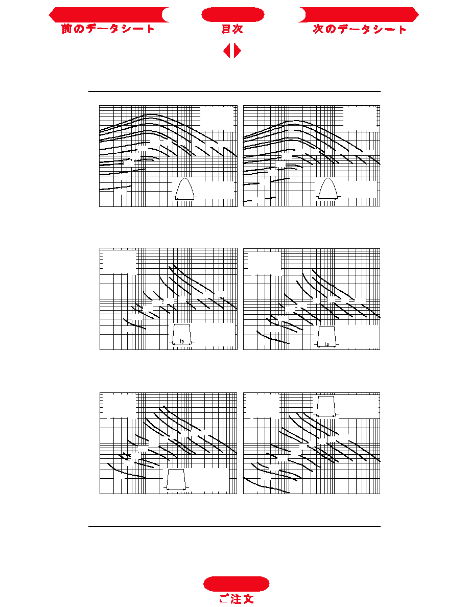
Fig. 7 - On-state Voltage Drop Characteristics
Fig. 8 - Thermal Impedance Z
thJC
Characteristic
Fig. 10 - Reverse Recovery Current Characteristics
Fig. 9 - Reverse Recovered Charge Characteristics
Fig. 6 - Maximum Non-repetitive Surge Current
Fig. 5 - Maximum Non-repetitive Surge Current
To Order
Next Data Sheet
Index
Previous Datasheet
ST223S Series
D-488
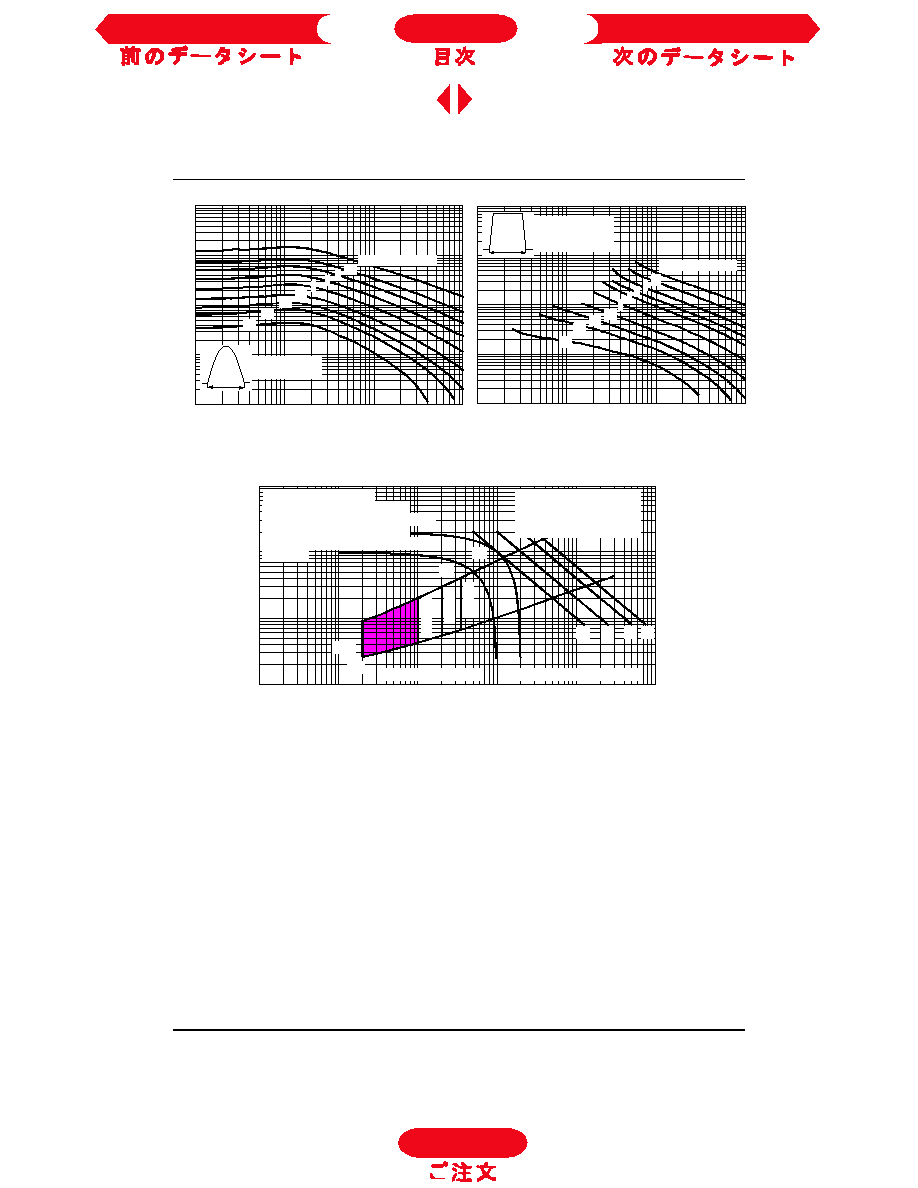
Fig. 13 - Frequency Characteristics
Fig. 11 - Frequency Characteristics
Fig. 12 - Frequency Characteristics
To Order
Next Data Sheet
Index
Previous Datasheet
ST223S Series
D-489
Fig. 14 - Maximum On-state Energy Power Loss Characteristics
Fig. 15 - Gate Characteristics
To Order
Next Data Sheet
Index
Previous Datasheet
ST223S Series
D-483
V
TM
Max. peak on-state voltage
1.58
I
TM
= 600A, T
J
= T
J
max, t
p
= 10ms sine wave pulse
V
T(TO)1
Low level value of threshold
voltage
V
T(TO)2
High level value of threshold
voltage
r
t
1
Low level value of forward
slope resistance
r
t
2
High level value of forward
slope resistance
I
H
Maximum holding current
600
T
J
= 25�C, I
T
> 30A
I
L
Typical latching current
1000
T
J
= 25�C, V
A
= 12V, Ra = 6
,
I
G
= 1A
Parameter
ST223S
Units
Conditions
On-state Conduction
1.05
(16.7% x
x I
T(AV)
< I <
x I
T(AV)
), T
J
= T
J
max.
1.09
(I >
x I
T(AV)
), T
J
= T
J
max.
V
0.88
(16.7% x
x I
T(AV)
< I <
x I
T(AV)
), T
J
= T
J
max.
0.82
(I >
x I
T(AV)
), T
J
= T
J
max.
m
mA
di/dt
Max. non-repetitive rate of rise
T
J
= T
J
max, V
DRM
= rated V
DRM
of turned-on current
I
TM
= 2 x di/dt
T
J
= 25�C, V
DM
= rated V
DRM
,
I
TM
= 50A DC, t
p
= 1�s
Resistive load, Gate pulse: 10V, 5
source
T
J
= T
J
max,
I
TM
= 300A, commutating di/dt
= 20A/�s
V
R
= 50V, t
p
= 500�s, dv/dt: see table in device code
Switching
Parameter
ST223S
Units
Conditions
1000
A/�s
t
d
Typical delay time
0.78
�s
Min
Max
dv/dt
Maximum critical rate of rise of
T
J
= T
J
max., linear to 80% V
DRM
, higher value
off-state voltage
available on request
I
RRM
Max. peak reverse and off-state
I
DRM
leakage current
Parameter
ST223S
Units
Conditions
Blocking
500
V/
�
s
40
mA
T
J
= T
J
max., rated V
DRM
/V
RRM
applied
P
GM
Maximum peak gate power
60
P
G(AV)
Maximum average gate power
10
I
GM
Max. peak positive gate current
10
A
T
J
= T
J
max, t
p
5ms
+V
GM
Maximum peak positive
gate voltage
-V
GM
Maximum peak negative
gate voltage
I
GT
Max. DC gate current required
to trigger
V
GT
Max. DC gate voltage required
to trigger
I
GD
Max. DC gate current not to trigger
20
mA
V
GD
Max. DC gate voltage not to trigger
0.25
V
Triggering
Parameter
ST223S
Units
Conditions
20
5
V
T
J
= T
J
max, t
p
5ms
200
mA
3
V
T
J
= 25�C, V
A
= 12V, Ra = 6
T
J
= T
J
max, rated V
DRM
applied
t
q
Max. turn-off time
10
20
W
T
J
= T
J
max, f = 50Hz, d% = 50
To Order
Next Data Sheet
Index
Previous Datasheet
ST223S Series
D-484
T
J
Max. junction operating temperature range
-40 to 125
T
stg
Max. storage temperature range
-40 to 150
R
thJC
Max. thermal resistance, junction to case
0.105
DC operation
R
thCS
Max. thermal resistance, case to heatsink
0.04
Mounting surface, smooth, flat and greased
T
Mounting torque, � 10%
31
Nm
(275)
(Ibf-in)
24.5
Nm
(210)
(Ibf-in)
wt
Approximate weight
280
g
Case style
TO-209AB (TO-93)
See Outline Table
Parameter
ST223S
Units
Conditions
Thermal and Mechanical Specifications
�C
K/W
Non lubricated threads
Lubricated threads
Ordering Information Table
180�
0.016
0.012
120�
0.019
0.020
90�
0.025
0.027
K/W
T
J
= T
J
max.
60�
0.036
0.037
30�
0.060
0.060
Conduction angle
Sinusoidal conduction
Rectangular conduction Units
Conditions
R
thJC
Conduction
(The following table shows the increment of thermal resistence R
thJC
when devices operate at different conduction angles than DC)
Device Code
5
6
8
9
ST
22
3
S
08
P
F
N
0
3
4
10
7
1
2
1
- Thyristor
2
- Essential part number
3
- 3 = Fast turn off
4
- S = Compression bonding Stud
5
- Voltage code: Code x 100 = V
RRM
(See Voltage Ratings table)
6
- P = Stud base 3/4" 16UNF-2A
M = Stud base metric threads M16 x 1.5
7
- Reapplied dv/dt code (for t
q
test condition)
8
- t
q
code
9
- 0 = Eyelet terminals (Gate and Aux. Cathode Leads)
1 = Fast-on terminals (Gate and Aux. Cathode Leads)
2 = Flag terminals (For Cathode and Gate Terminals)
- Critical dv/dt:
None = 500V/�sec (Standard value)
L
= 1000V/�sec (Special selection)
dv/dt - t
q
combinations available
dv/dt (V/�s)
20
50
100
200
400
10
CN
DN
EN
FN *
--
12
CM
DM
EM
FM
--
15
CL
DL
EL
FL *
HL
18
CP
DP
EP
FP
HP
20
CK
DK
EK
FK
HK
25
--
--
--
--
HJ
30
--
--
--
--
HH
t
q
(�s)
*
Standard part number.
All other types available only on request.
10
To Order
Next Data Sheet
Index
Previous Datasheet
ST223S Series
D-485
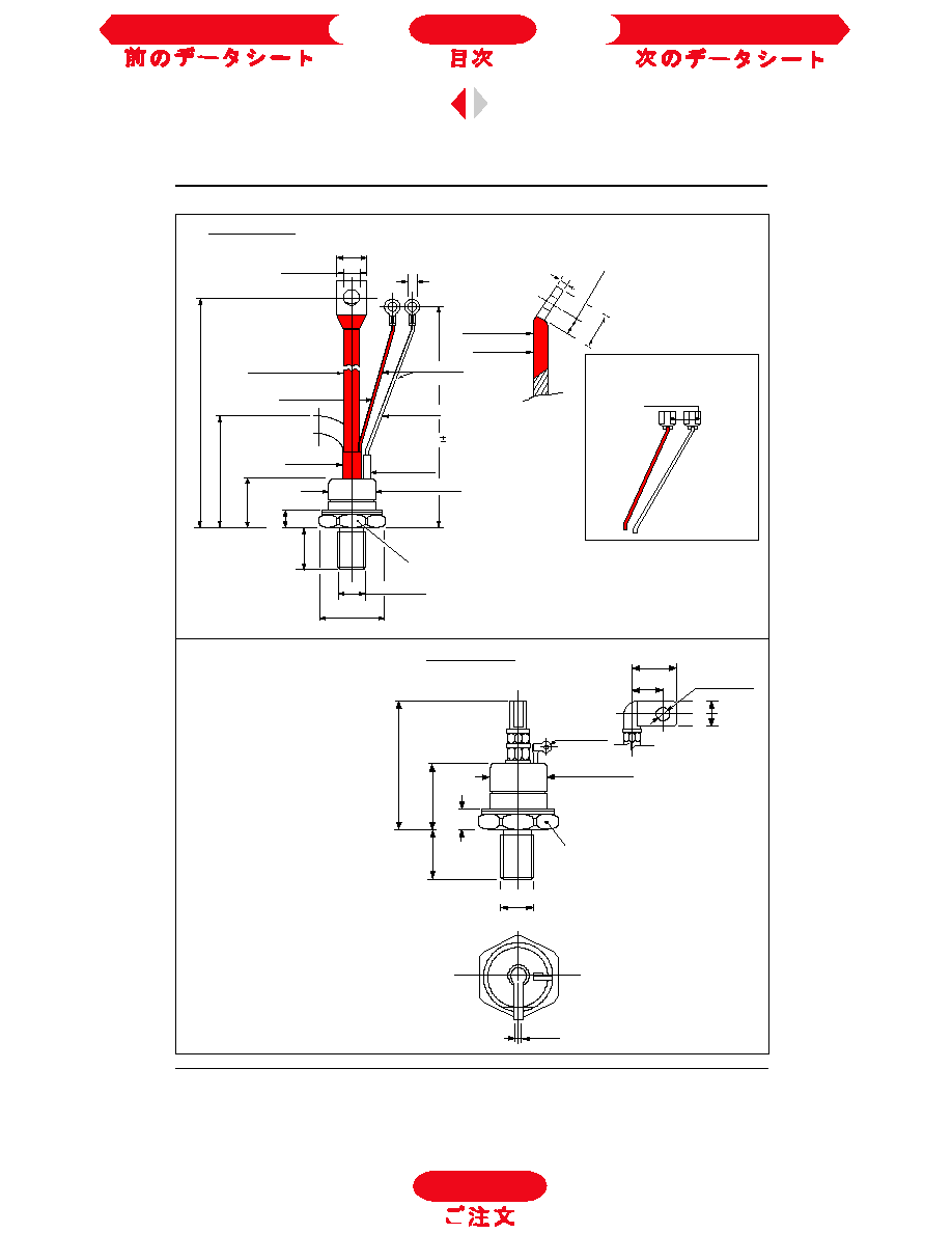
Case Style TO-209AB (TO-93)
All dimensions in millimeters (inches)
Fast-on Terminals
Outline Table
C.S. 0.4 mm
2
10 (0.39)
RED SHRINK
RED CATHODE
RED SILICON RUBBER
4.3 (0.17) DIA
2
1
(
0
.
8
3
)
1
2
.
5
(
0
.
4
9
)
M
A
X
.
1
5
7
(
6
.
1
8
)
1
7
0
(
6
.
6
9
)
(.0006 s.i.)
8.5 (0.33) DIA.
16.5 (0.65) MAX.
M
A
X
.
7
0
(
2
.
7
5
)
M
I
N
.
CERAMIC HOUSING
22.5 (0.88) MAX. DIA.
2
9
(
1
.
1
4
)
M
A
X
.
SW 27
C.S. 16mm
2
FLEXIBLE LEAD
(.025 s.i.)
2.6 (0.10) MAX.
WHITE SHRINK
2
0
(0
.7
9
)
M
IN
.
29.5 (1.16)
MAX.
1/2"-20UNF-2A
9
.5
(
0
.3
7)
M
IN
.
WHITE GATE
215 (8.46)
Case Style TO-209AB (TO-93) Flag
All dimensions in millimeters (inches)
CERAMIC HOUSING
2
7
.
5
(
1
.
0
8
)
M
A
X
.
3
8
.
5
(
1
.
5
2
)
M
A
X
.
3 (0.12)
8
0
(
3
.
1
5
)
M
A
X
.
DIA. 27.5 (1.08) MAX.
1
6
(
0
.
6
3
)
M
A
X
.
FLAG TERMINALS
1.5 (0.06) DIA.
SW 32
22 (0.89)
DIA. 6.5 (0.25)
1
3
(
0
.
5
1
)
14 (0.55)
*FOR METRIC DEVICE. M16 X 1.5 - LENGHT 21 (0.83) MAX.
3/4"-16UNF-2A*
AMP. 280000-1
REF-250
To Order
Next Data Sheet
Index
Previous Datasheet