 | –≠–ª–µ–∫—Ç—Ä–æ–Ω–Ω—ã–π –∫–æ–º–ø–æ–Ω–µ–Ω—Ç: ST230CC | –°–∫–∞—á–∞—Ç—å:  PDF PDF  ZIP ZIP |
Features
Center amplifying gate
Metal case with ceramic insulator
International standard case TO-200AB (A-PUK)
Typical Applications
DC motor controls
Controlled DC power supplies
AC controllers
I
T(AV)
410
A
@ T
hs
55
∞C
I
T(RMS)
780
A
@ T
hs
25
∞C
I
TSM
@
50Hz
5700
A
@ 60Hz
5970
A
I
2
t
@
50Hz
163
KA
2
s
@ 60Hz
149
KA
2
s
V
DRM
/V
RRM
400 to 2000
V
t
q
typical
100
µs
T
J
- 40 to 125
∞C
Parameters
ST230C..C
Units
Major Ratings and Characteristics
case style TO-200AB (A-PUK)
410A
PHASE CONTROL THYRISTORS
Hockey Puk Version
ST230C..C SERIES
1
Bulletin I25162 rev. D 04/03
www.irf.com
ST230C..C Series
2
Bulletin I25162 rev. D 04/03
www.irf.com
di/dt
Max. non-repetitive rate of rise
Gate drive 20V, 20
, t
r
1µs
of turned-on current
T
J
= T
J
max, anode voltage
80% V
DRM
Gate current 1A, di
g
/dt = 1A/µs
V
d
= 0.67% V
DRM
,
T
J
= 25∞C
I
TM
= 300A, T
J
= T
J
max, di/dt
= 20A/µs, V
R
= 50V
dv/dt
= 20V/µs, Gate 0V 100
,
t
p
= 500µs
Parameter
ST230C..C
Units Conditions
Switching
1000
A/µs
t
d
Typical delay time
1.0
t
q
Typical turn-off time
100
µs
I
T(AV)
Max. average on-state current
410 (165)
A
180∞ conduction, half sine wave
@ Heatsink temperature
55 (85)
∞C
double side (single side) cooled
I
T(RMS)
Max. RMS on-state current
780
DC @ 25∞C heatsink temperature double side cooled
I
TSM
Max. peak, one-cycle
5700
t = 10ms
No voltage
non-repetitive surge current
5970
A
t = 8.3ms
reapplied
4800
t = 10ms
100% V
RRM
5000
t = 8.3ms
reapplied
Sinusoidal half wave,
I
2
t
Maximum I
2
t for fusing
163
t = 10ms
No voltage
Initial T
J
= T
J
max.
148
t = 8.3ms
reapplied
115
t = 10ms
100% V
RRM
105
t = 8.3ms
reapplied
I
2
t
Maximum I
2
t for fusing
1630
KA
2
s
t = 0.1 to 10ms, no voltage reapplied
V
T(TO)
1
Low level value of threshold
voltage
V
T(TO)
2
High level value of threshold
voltage
r
t1
Low level value of on-state
slope resistance
r
t2
High level value of on-state
slope resistance
V
TM
Max. on-state voltage
1.69
V
I
pk
= 880A, T
J
= T
J
max, t
p
= 10ms sine pulse
I
H
Maximum holding current
600
I
L
Max. (typical) latching current
1000 (300)
0.92
(16.7% x
x I
T(AV)
< I <
x I
T(AV)
), T
J
= T
J
max.
0.88
(16.7% x
x I
T(AV)
< I <
x I
T(AV)
), T
J
= T
J
max.
0.81
(I >
x I
T(AV)
),T
J
= T
J
max.
Parameter
ST230C..C
Units Conditions
0.98
(I >
x I
T(AV)
),T
J
= T
J
max.
On-state Conduction
KA
2
s
V
m
mA
T
J
= 25∞C, anode supply 12V resistive load
Voltage
V
DRM
/V
RRM
, max. repetitive
V
RSM
, maximum non-
I
DRM
/I
RRM
max.
Type number
Code
peak and off-state voltage
repetitive peak voltage
@ T
J
= T
J
max
V
V
mA
04
400
500
08
800
900
ST230C..C
12
1200
1300
30
14
1400
1500
16
1600
1700
18
1800
1900
20
2000
2100
ELECTRICAL SPECIFICATIONS
Voltage Ratings
ST230C..C Series
3
Bulletin I25162 rev. D 04/03
www.irf.com
dv/dt
Maximum critical rate of rise of
off-state voltage
I
DRM
Max. peak reverse and off-state
I
RRM
leakage current
Blocking
500
V/
µ
s
T
J
= T
J
max. linear to 80% rated V
DRM
Parameter
ST230C..C
Units Conditions
30
mA
T
J
= T
J
max, rated V
DRM
/V
RRM
applied
P
GM
Maximum peak gate power
10.0
T
J
= T
J
max, t
p
5ms
P
G(AV)
Maximum average gate power
2.0
T
J
= T
J
max, f = 50Hz, d% = 50
I
GM
Max. peak positive gate current
3.0
A
T
J
= T
J
max, t
p
5ms
+V
GM
Maximum peak positive
gate voltage
-V
GM
Maximum peak negative
gate voltage
T
J
= - 40∞C
mA
T
J
= 25∞C
T
J
= 125∞C
T
J
= - 40∞C
V
T
J
= 25∞C
T
J
= 125∞C
I
GD
DC gate current not to trigger
10
mA
Parameter
ST230C..C
Units Conditions
20
5.0
Triggering
TYP.
MAX.
180
-
90
150
40
-
2.9
-
1.8
3.0
1.2
-
V
GD
DC gate voltage not to trigger
0.25
V
Max. gate current/voltage not to
trigger is the max. value which
will not trigger any unit with rated
V
DRM
anode-to-cathode applied
T
J
= T
J
max
Max. required gate trigger/ cur-
rent/ voltage are the lowest value
which will trigger all units 12V
anode-to-cathode applied
V
GT
DC gate voltage required
to trigger
I
GT
DC gate current required
to trigger
W
V
T
J
= T
J
max, t
p
5ms
T
J
Max. operating temperature range
-40 to 125
T
stg
Max. storage temperature range
-40 to 150
R
thJ-hs
Max. thermal resistance,
0.17
DC operation single side cooled
junction to heatsink
0.08
DC operation double side cooled
R
thC-hs
Max. thermal resistance,
0.033
DC operation single side cooled
case to heatsink
0.017
DC operation double side cooled
F
Mounting force, ± 10%
4900
N
(500)
(Kg)
wt
Approximate weight
50
g
Parameter
ST230C..C
Units
Conditions
K/W
Thermal and Mechanical Specification
∞C
Case style
TO - 200AB (A-PUK)
See Outline Table
K/W
ST230C..C Series
4
Bulletin I25162 rev. D 04/03
www.irf.com
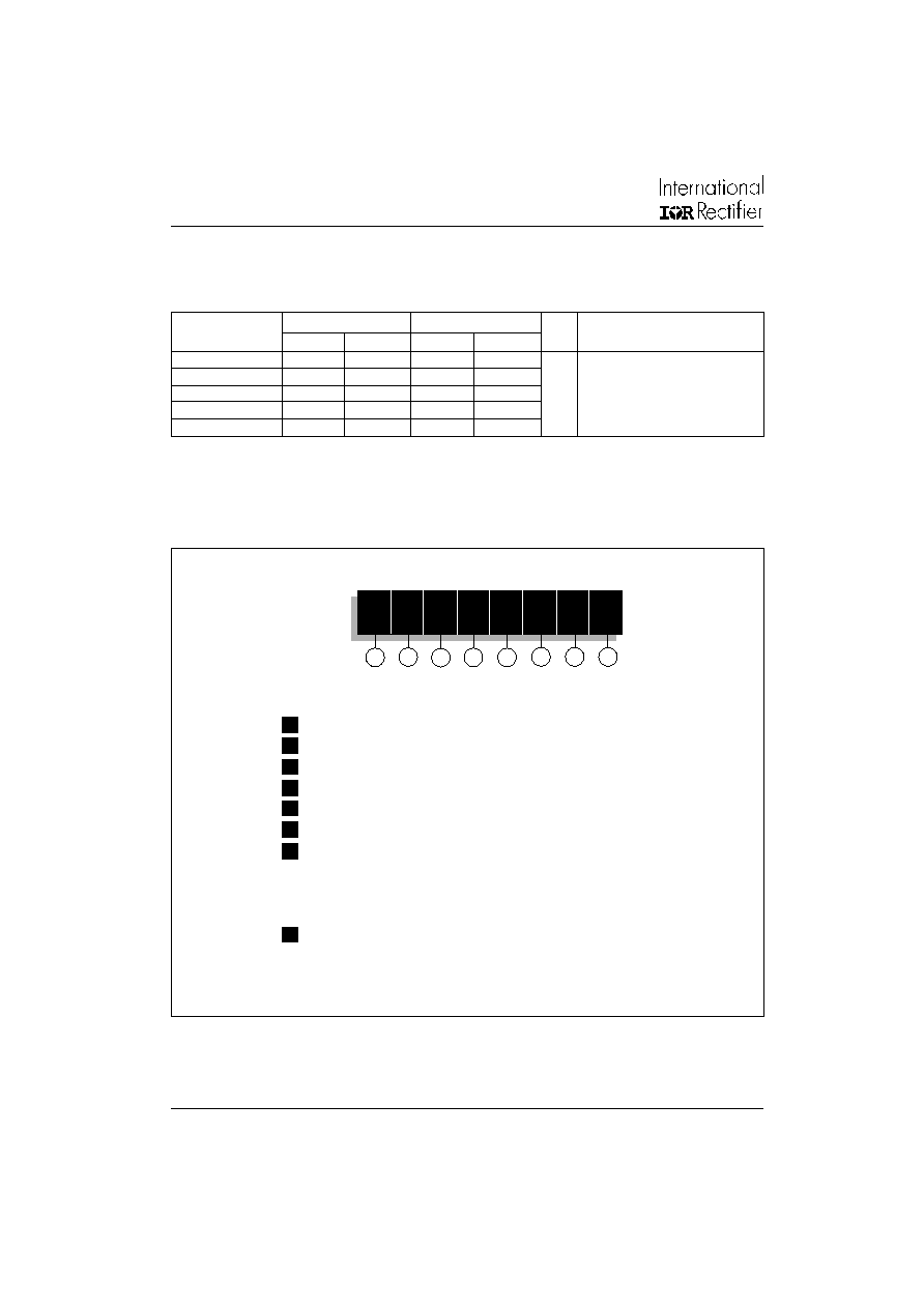
1
-
Thyristor
2
-
Essential part number
3
-
0 = Converter grade
4
-
C = Ceramic Puk
5
-
Voltage code: Code x 100 = V
RRM
(See Voltage Rating Table)
6
-
C = Puk Case TO-200AB (A-PUK)
7
-
0 = Eyelet terminals (Gate and Auxiliary Cathode Unsoldered Leads)
1 = Fast-on terminals (Gate and Auxiliary Cathode Unsoldered Leads)
2 = Eyelet terminals (Gate and Auxiliary Cathode Soldered Leads)
3 = Fast-on terminals (Gate and Auxiliary Cathode Soldered Leads)
8
-
Critical dv/dt: None = 500V/µsec (Standard selection)
L
= 1000V/µsec (Special selection)
Ordering Information Table
R
thJ-hs
Conduction
(The following table shows the increment of thermal resistence R
thJ-hs
when devices operate at different conduction angles than DC)
Device Code
5
3
4
ST
23
0
C
20
C
1
7
6
8
1
2
Single Side Double Side
Single Side Double Side
180∞
0.015
0.017
0.011
0.011
T
J
= T
J
max.
120∞
0.018
0.019
0.019
0.019
90∞
0.024
0.024
0.026
0.026
K/W
60∞
0.035
0.035
0.036
0.037
30∞
0.060
0.060
0.060
0.061
Sinusoidal conduction Rectangular conduction
Conduction angle
Units
Conditions
ST230C..C Series
5
Bulletin I25162 rev. D 04/03
www.irf.com
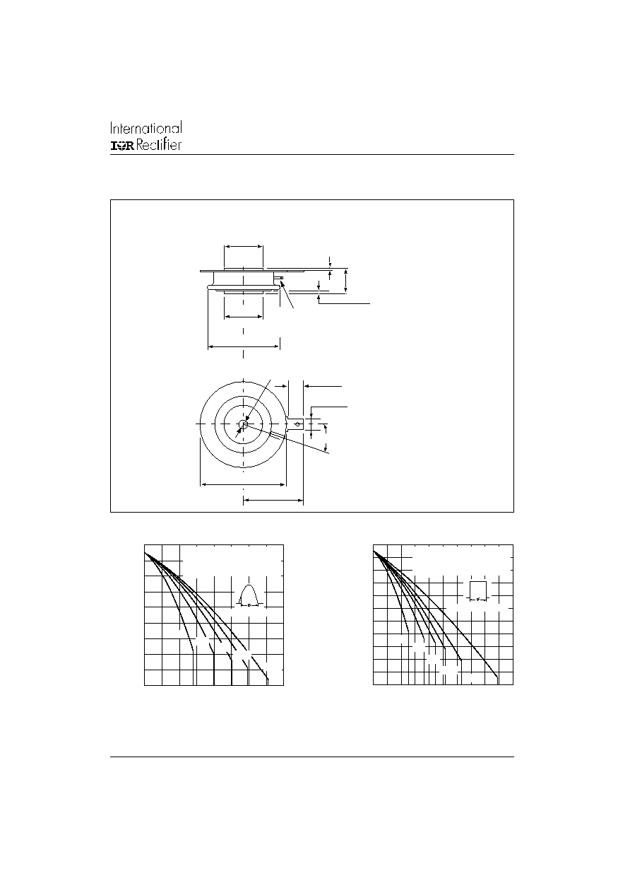
Outline Table
Case Style TO-200AB (A-PUK)
All dimensions in millimeters (inches)
Fig. 1 - Current Ratings Characteristics
Fig. 2 - Current Ratings Characteristics
DIA. MAX.
4.75 (0.19)
28 (1.10)
6.5 (0.26)
19 (0.75)
0.3 (0.01) MIN.
0.3 (0.01) MIN.
13.7 / 14.4
(0.54 / 0.57)
25∞± 5∞
GATE TERM. FOR
1.47 (0.06) DIA.
PIN RECEPTACLE
ANODE TO GATE
CREEPAGE DISTANCE: 7.62 (0.30) MIN.
STRIKE DISTANCE: 7.12 (0.28) MIN.
19 (0.75)
DIA. MAX.
38 (1.50) DIA MAX.
2 HOLES 3.56 (0.14) x
1.83 (0.07) MIN. DEEP
42 (1.65) MAX.
Quote between upper and lower
pole pieces has to be considered
after application of Mounting Force
(see Thermal and Mechanical
Specification)
Average On-state Current (A)
Average On-state Current (A)
Maximum Allowable Heatsink Temperature (
∞
C)
Maximum Allowable Heatsink Temperature (
∞
C)
40
50
60
70
80
90
00
10
20
30
0
40
80 120 160 200 240 280 320
30∞
60∞
90∞
120∞
180∞
Conduction Angle
ST230C..C Series
(Single Side Cooled)
R (DC) = 0.17 K/W
thJ-hs
20
30
40
50
60
70
80
90
00
10
20
30
0
100
200
300
400
500
DC
30∞
60∞
90∞
120∞
180∞
Conduction Period
ST230C..C Series
(Single Side Cooled)
R (DC) = 0.17 K/W
thJ-hs