230A
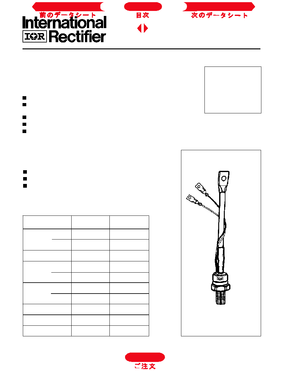
PHASE CONTROL THYRISTORS
Stud Version
ST230S SERIES
Bulletin I25163/B
Features
Center amplifying gate
Hermetic metal case with ceramic insulator
(Also available with glass-metal seal up to 1200V)
International standard case TO-209AB (TO-93)
Threaded studs UNF 3/4 - 16UNF2A or ISO M16x1.5
Compression Bonded Encapsulation for heavy duty
operations such as severe thermal cycling
Typical Applications
DC motor controls
Controlled DC power supplies
AC controllers
I
T(AV)
230
A
@ T
C
85
°C
I
T(RMS)
360
A
I
TSM
@
50Hz
5700
A
@ 60Hz
5970
A
I
2
t
@
50Hz
163
KA
2
s
@ 60Hz
149
KA
2
s
V
DRM
/V
RRM
400 to 1600
V
t
q
typical
100
µs
T
J
- 40 to 125
°C
Parameters
ST230S
Units
Major Ratings and Characteristics
case style
TO-209AB (TO-93)
Next Data Sheet
Index
Previous Datasheet
To Order
ST230S Series
2222222222222
12
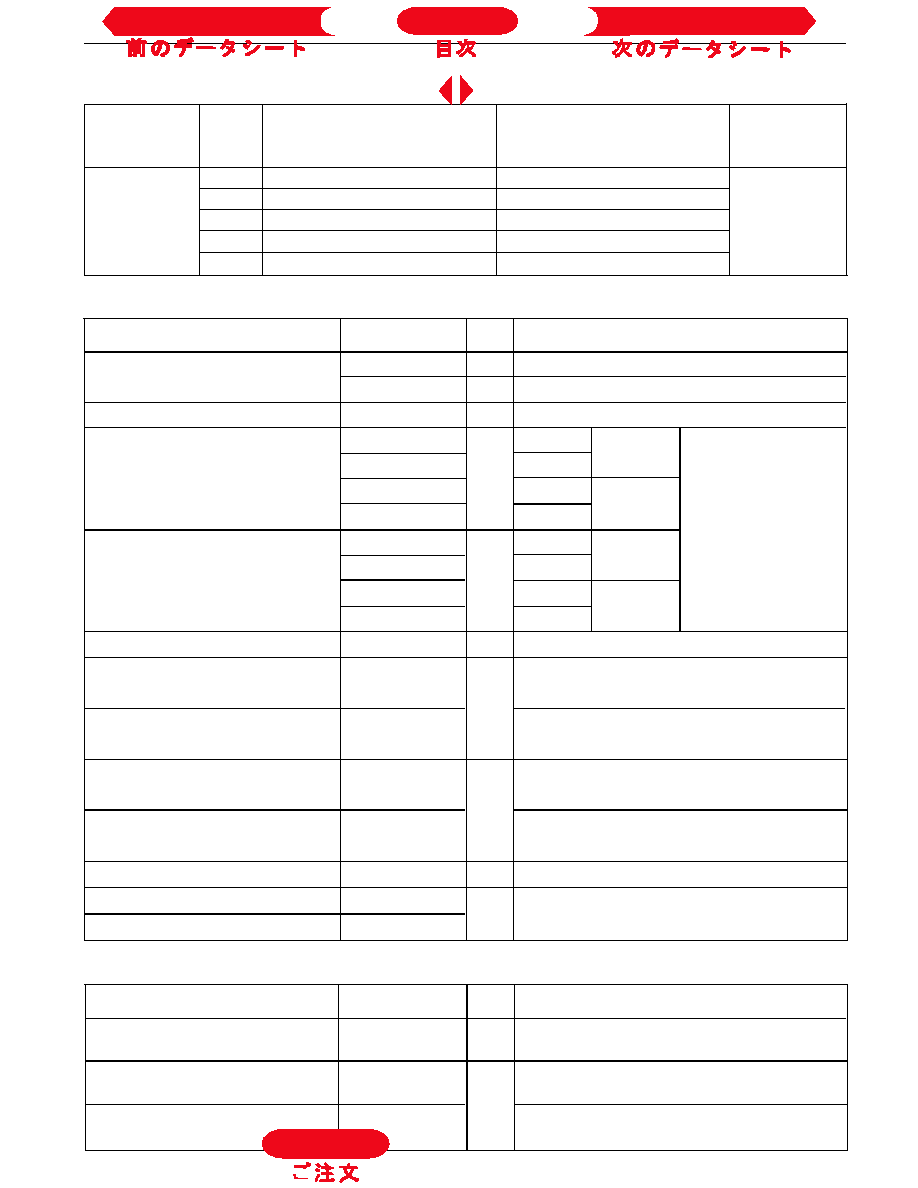
ELECTRICAL SPECIFICATIONS
Voltage Ratings
Voltage
V
DRM
/V
RRM
, max. repetitive
V
RSM
, maximum non-
I
DRM
/I
RRM
max.
Type number
Code
peak and off-state voltage
repetitive peak voltage
@ T
J
= T
J
max
V
V
mA
04
400
500
08
800
900
ST230S
12
1200
1300
30
14
1400
1500
16
1600
1700
I
T(AV)
Max. average on-state current
230
A
180° conduction, half sine wave
@ Case temperature
85
°C
I
T(RMS)
Max. RMS on-state current
360
A
DC @ 78°C case temperature
I
TSM
Max. peak, one-cycle
5700
t = 10ms
No voltage
non-repetitive surge current
5970
t = 8.3ms
reapplied
4800
t = 10ms
100% V
RRM
5000
t = 8.3ms
reapplied
Sinusoidal half wave,
I
2
t
Maximum I
2
t for fusing
163
t = 10ms
No voltage
Initial T
J
= T
J
max.
148
t = 8.3ms
reapplied
115
t = 10ms
100% V
RRM
105
t = 8.3ms
reapplied
I
2
t
Maximum I
2
t for fusing
1630
KA
2
s
t = 0.1 to 10ms, no voltage reapplied
V
T(TO)1
Low level value of threshold
voltage
V
T(TO)2
High level value of threshold
voltage
r
t
1
Low level value of on-state
slope resistance
r
t
2
High level value of on-state
slope resistance
V
TM
Max. on-state voltage
1.55
V
I
pk
= 720A, T
J
= T
J
max, t
p
= 10ms sine pulse
I
H
Maximum holding current
600
I
L
Max. (typical) latching current
1000 (300)
0.92
(16.7% x
x I
T(AV)
< I <
x I
T(AV)
), T
J
= T
J
max.
0.88
(16.7% x
x I
T(AV)
< I <
x I
T(AV)
), T
J
= T
J
max.
0.81
(I >
x I
T(AV)
),T
J
= T
J
max.
Parameter
ST230S
Units Conditions
0.98
(I >
x I
T(AV)
),T
J
= T
J
max.
On-state Conduction
KA
2
s
V
m
mA
T
J
= 25°C, anode supply 12V resistive load
A
di/dt
Max. non-repetitive rate of rise
Gate drive 20V, 20
, t
r
1µs
of turned-on current
T
J
= T
J
max, anode voltage
80%
V
DRM
Gate current 1A, di
g
/dt = 1A/µs
V
d
= 0.67% V
DRM
,
T
J
= 25°C
I
TM
= 300A, T
J
= T
J
max, di/dt
= 20A/µs, V
R
= 50V
dv/dt
= 20V/µs, Gate 0V 100
,
t
p
= 500µs
Parameter
ST230S
Units Conditions
1000
A/µs
Switching
t
q
Typical turn-off time
100
µs
t
d
Typical delay time
1.0
To Order
Next Data Sheet
Index
Previous Datasheet
ST230S Series
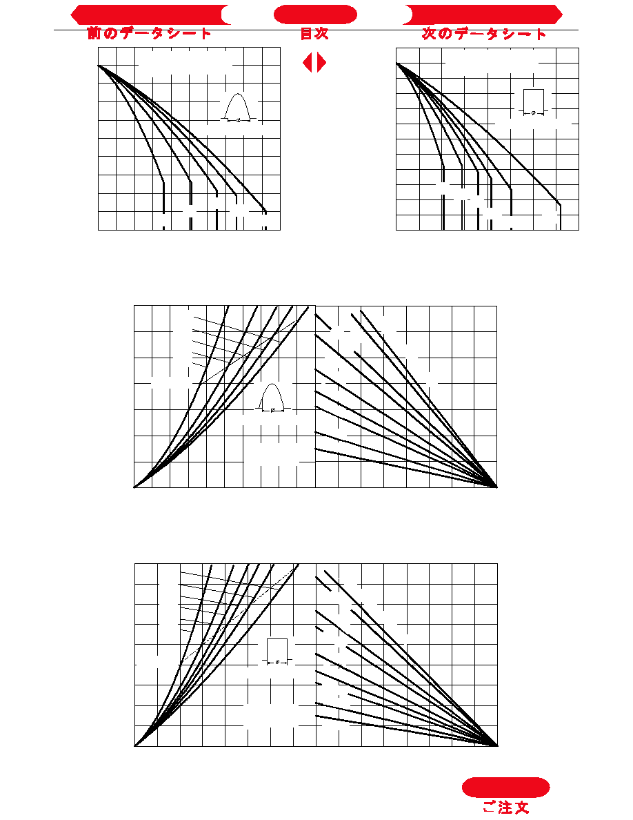
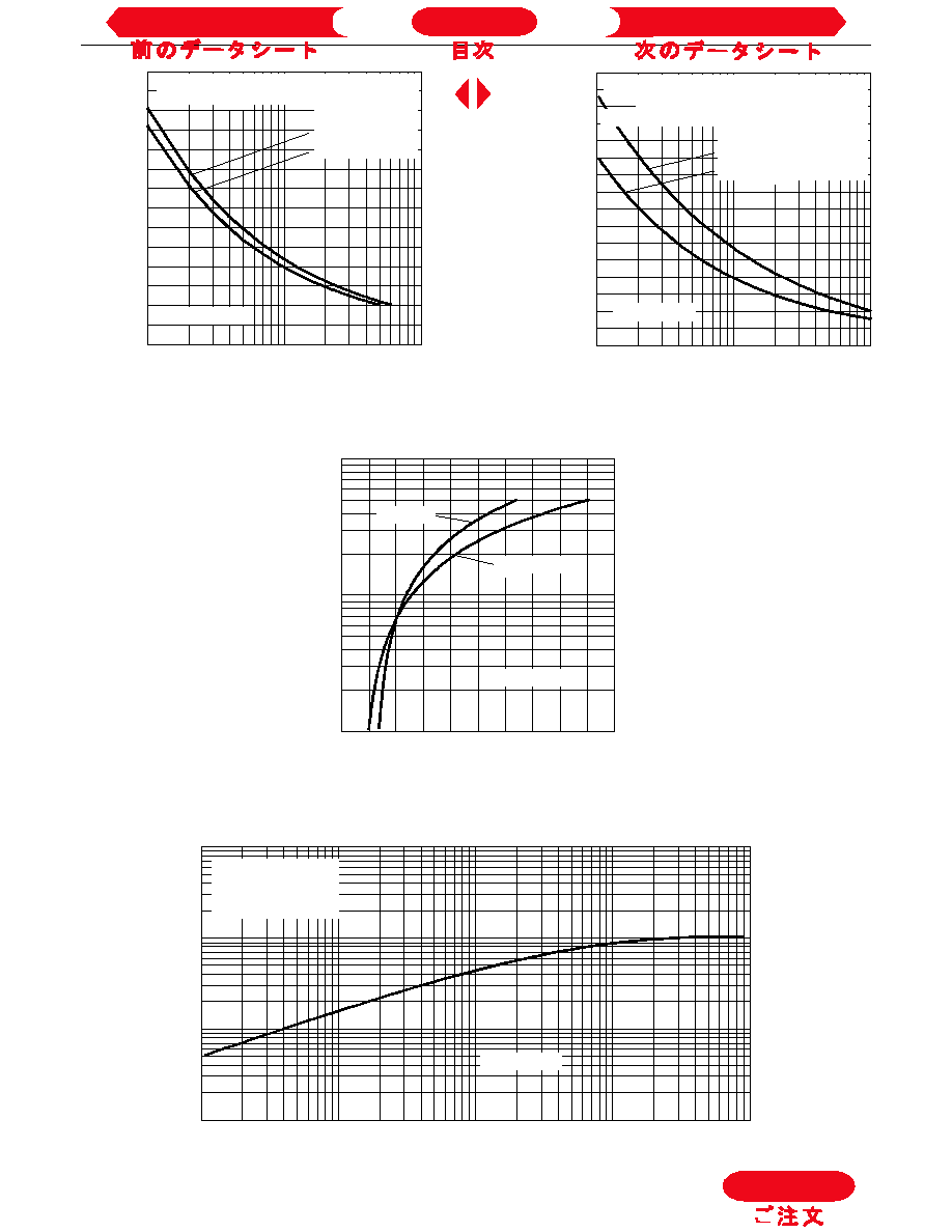
Fig. 2 - Current Ratings Characteristics
Fig. 1 - Current Ratings Characteristics
Fig. 4 - On-state Power Loss Characteristics
Fig. 3 - On-state Power Loss Characteristics
To Order
Next Data Sheet
Index
Previous Datasheet
ST230S Series
Fig. 8 - Thermal Impedance Z
thJC
Characteristic
Fig. 7 - On-state Voltage Drop Characteristics
Fig. 6 - Maximum Non-Repetitive Surge Current
Fig. 5 - Maximum Non-Repetitive Surge Current
To Order
Next Data Sheet
Index
Previous Datasheet