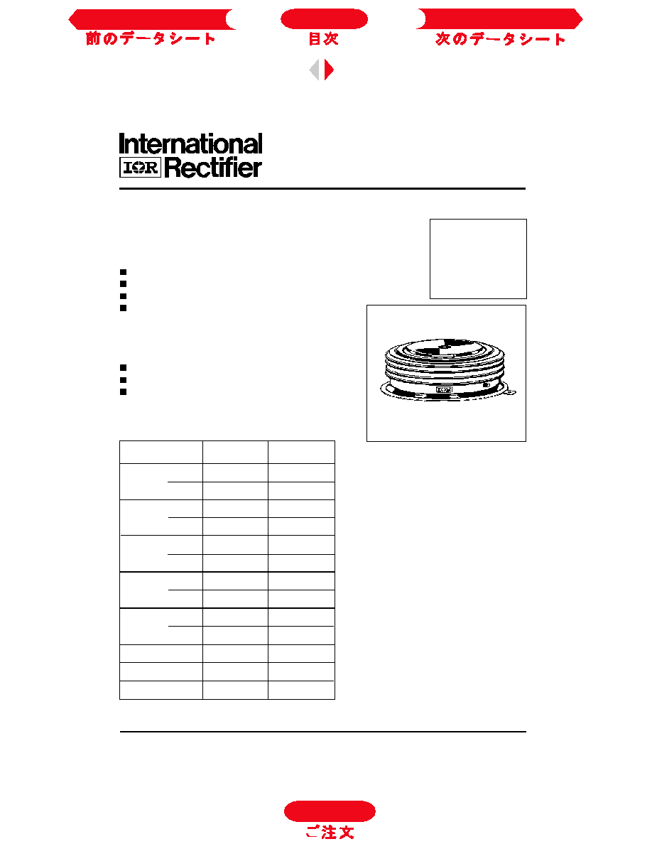
ST2600C..R Series
2222222222222
12
D-420
Voltage
V
DRM
/V
RRM
, max. repetitive
V
RSM
, maximum non-
I
DRM
/I
RRM
max.
Type number
Code
peak and off-state voltage
repetitive peak voltage
@ T
C
= 125°C
V
V
mA
20
2000
2100
22
2200
2300
24
2400
2500
26
2600
2700
28
2800
2900
30
3000
3100
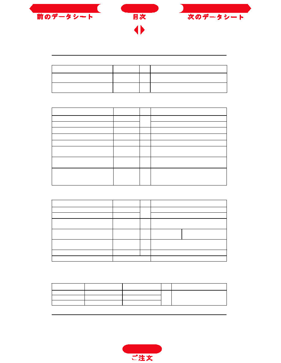
ELECTRICAL SPECIFICATIONS
Voltage Ratings
Parameter
ST2600C..R
Units Conditions
Switching
di/dt
Max. repetitive 50Hz (no repetitive)
From 67% V
DRM
gate drive 20V, 20
, t
r
=
1µs
rate of rise of turned-on current
T
J
= T
J
max.
Gate drive 30V, 15
,
V
d
= 67% V
DRM
,
T
J
= 25°C
Rise time 0.5µs
I
T
= 800A, t
p
= 1ms, T
J
= T
J
max, V
RM
= 50V,
dI
RR
/dt = 20A/µs, V
DR
=
67% V
DRM
,
dV/dt
= 20V/µs linear
150 (300)
A/µs
µs
t
q
Typical turn-off time
400
t
d
Maximum delay time
2.0
I
T(AV)
Max. average on-state current
2220 (1440)
A
@ Case temperature
80
°C
I
T(AV)
Max. average on-state current
2630 (1160)
A
@ Heatsink temperature
55 (85)
°C
I
T(RMS)
Max. RMS on-state current
4800
A
DC @ 25°C heatsink temperature double side cooled
I
TSM
Max. peak, one-cycle
No voltage
non-repetitive surge current
reapplied
50% V
RRM
reapplied
Sinusoidal half wave,
I
2
t
Maximum I
2
t for fusing
No voltage
Initial T
C
= 125°C
reapplied
50% V
RRM
reapplied
V
T(TO)
Max. value of threshold voltage
0.89
V
T
J
= T
J
max.
r
t
Max. value of on-state slope
resistance
V
TM
Max. on-state voltage
1.45
V
I
pk
= 2900A, T
C
= 25°C
I
L
Max. (typical) latching current
300 (100)
mA
T
J
= 25°C, V
D
=
5V
Parameter
ST2600C..R
Units
Conditions
On-state Conduction
A
KA
2
s
m
180° conduction, half sine wave
double side (single side [anode side]) cooled
t = 10ms
t = 8.3ms
t = 10ms
t = 8.3ms
t = 10ms
t = 8.3ms
t = 10ms
t = 8.3ms
46000
48200
36800
38500
10580
9640
6770
6150
ST2600C..R
250
0.19
T
J
= T
J
max.
Next Data Sheet
Index
Previous Datasheet
To Order
ST2600C..R Series
D-423
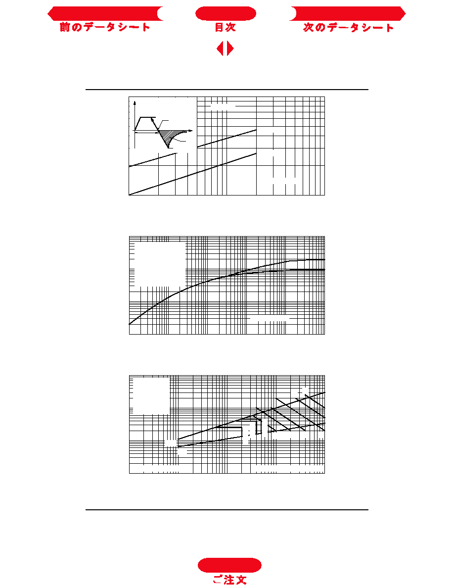
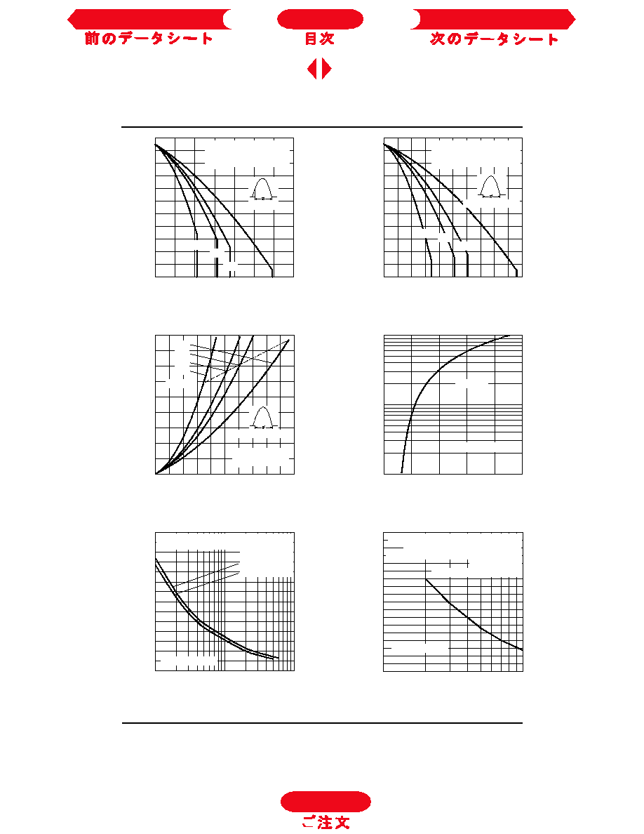
Fig. 1 - Current Ratings Characteristics
Fig. 2 - Current Ratings Characteristics
Fig. 5 - Maximum Non-Repetitive Surge Current
Fig. 6 - Maximum Non-Repetitive Surge Current
Fig. 3 - On-state Power Loss Characteristics
Fig. 4 - On-state Voltage Drop Characteristics
To Order
Next Data Sheet
Index
Previous Datasheet
ST2600C..R Series
23
D-421
3333
dv/dt
Maximum linear rate of rise of
off-state voltage
I
RRM
Max. peak reverse and off-state
I
DRM
leakage current
Blocking
500
V/µs
T
J
= T
J
max. to 67% rated V
DRM
Parameter
ST2600C..R
Units
Conditions
250
mA
T
J
= 125°C rated V
DRM
/V
RRM
applied
Triggering
P
GM
Maximum peak gate power
150
t
p
= 100µs
P
G(AV)
Maximum average gate power
10
I
GM
Max. peak positive gate current
30
A
Anode positive with respect to cathode
V
GM
Max. peak positive gate voltage
30
V
Anode positive with respect to cathode
-V
GM
Max. peak negative gate voltage
0.25
V
Anode negative with respect to cathode
I
GT
Maximum DC gate current
required to trigger
V
GT
Maximum gate voltage required
to trigger
Parameter
ST2600C..R
Units
Conditions
W
400
mA
T
C
= 25°C, V
DRM
= 5V
4
V
T
C
= 25°C, V
DRM
= 5V
V
GD
DC gate voltage not to trigger
0.25
V
T
C
= 125°C
Max. gate current/voltage not to
trigger is the max. value which
will not trigger any unit with rated
V
DRM
anode-to-cathode applied
180°
0.0010
0.0010
T
J
= T
J
max.
120°
0.0017
0.0017
K/W
60°
0.0044
0.0044
R
thJ-C
Conduction
(The following table shows the increment of thermal resistence R
thJ-C
when devices operate at different conduction angles than DC)
Conduction angle
Single side
Double side
Units
Conditions
T
J
max. Max. operating temperature
125
On-state (conducting)
T
stg
Max. storage temperature range
-55 to 125
R
thJ-C
Thermal resistance, junction
0.019
DC operation single side cooled
to case
0.0095
DC operation double side cooled
R
th(C-h)
Thermal resistance, case
0.004
Single side cooled
to heatsink
0.002
Double side cooled
F
Mounting force ± 10%
wt
Approximate weight
1600
g
Case style
(R-PUK)
See Outline Table
Parameter
ST2600C..R
Units
Conditions
Thermal and Mechanical Specification
°C
Clamping force 43KN with
mounting compound
43000
(4400)
N
(Kg)
K/W
K/W
To Order
Next Data Sheet
Index
Previous Datasheet