560A
PHASE CONTROL THYRISTORS
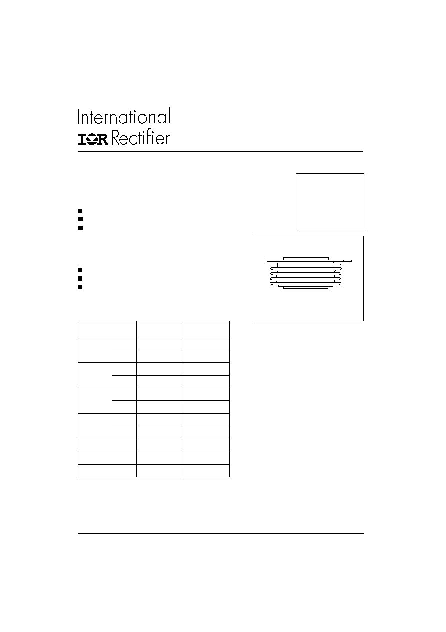
Hockey Puk Version
ST300C..L SERIES
1
Bulletin I25193 rev. B 04/00
www.irf.com
Features
Center amplifying gate
Metal case with ceramic insulator
International standard case TO-200AC (B-PUK)
Typical Applications
DC motor controls
Controlled DC power supplies
AC controllers
I
T(AV)
560
A
@ T
hs
55
∞C
I
T(RMS)
1115
A
@ T
hs
25
∞C
I
TSM
@
50Hz
8000
A
@ 60Hz
8380
A
I
2
t
@
50Hz
320
KA
2
s
@ 60Hz
292
KA
2
s
V
DRM
/V
RRM
400 to 2000
V
t
q
typical
100
µs
T
J
- 40 to 125
∞C
Parameters
ST300C..L
Units
Major Ratings and Characteristics
case style TO-200AC (B-PUK)
ST300C..L Series
2
www.irf.com
Bulletin I25193 rev. B 04/00
I
T(AV)
Max. average on-state current
560 (275)
A
180∞ conduction, half sine wave
@ Heatsink temperature
55 (75)
∞C
double side (single side) cooled
I
T(RMS)
Max. RMS on-state current
1115
DC @ 25∞C heatsink temperature double side cooled
I
TSM
Max. peak, one-cycle
8000
t = 10ms
No voltage
non-repetitive surge current
8380
A
t = 8.3ms
reapplied
6730
t = 10ms
100% V
RRM
7040
t = 8.3ms
reapplied
Sinusoidal half wave,
I
2
t
Maximum I
2
t for fusing
320
t = 10ms
No voltage
Initial T
J
= T
J
max.
292
t = 8.3ms
reapplied
226
t = 10ms
100% V
RRM
207
t = 8.3ms
reapplied
I
2
t
Maximum I
2
t for fusing
3200
KA
2
s t = 0.1 to 10ms, no voltage reapplied
V
T(TO)
1
Low level value of threshold
voltage
V
T(TO)
2
High level value of threshold
voltage
r
t1
Low level value of on-state
slope resistance
r
t2
High level value of on-state
slope resistance
V
TM
Max. on-state voltage
2.18
V
I
pk
= 1635A, T
J
= T
J
max, t
p
= 10ms sine pulse
I
H
Maximum holding current
600
I
L
Typical latching current
1000
ELECTRICAL SPECIFICATIONS
Voltage Ratings
Voltage
V
DRM
/V
RRM
, max. repetitive
V
RSM
, maximum non-
I
DRM
/I
RRM
max.
Type number
Code
peak and off-state voltage
repetitive peak voltage
@ T
J
= T
J
max
V
V
mA
04
400
500
08
800
900
12
1200
1300
16
1600
1700
18
1800
1900
20
2000
2100
ST300C..L
50
0.97
(16.7% x
x I
T(AV)
< I <
x I
T(AV)
), T
J
= T
J
max.
0.74
(16.7% x
x I
T(AV)
< I <
x I
T(AV)
), T
J
= T
J
max.
0.73
(I >
x I
T(AV)
),T
J
= T
J
max.
Parameter
ST300C..L
Units Conditions
0.98
(I >
x I
T(AV)
),T
J
= T
J
max.
On-state Conduction
KA
2
s
V
m
mA
T
J
= 25∞C, anode supply 12V resistive load
ST300C..L Series
3
www.irf.com
Bulletin I25193 rev. B 04/00
di/dt
Max. non-repetitive rate of rise
Gate drive 20V, 20
, t
r
1µs
of turned-on current
T
J
= T
J
max, anode voltage
80% V
DRM
Gate current 1A, di
g
/dt = 1A/µs
V
d
= 0.67% V
DRM
,
T
J
= 25∞C
I
TM
= 550A, T
J
= T
J
max, di/dt
= 40A/µs, V
R
= 50V
dv/dt
= 20V/µs, Gate 0V 100
, t
p
= 500µs
Parameter
ST300C..L
Units Conditions
t
d
Typical delay time
1.0
Switching
t
q
Typical turn-off time
100
µs
1000
A/µs
dv/dt
Maximum critical rate of rise of
off-state voltage
I
RRM
Max. peak reverse and off-state
I
DRM
leakage current
Blocking
500
V/
µs
T
J
= T
J
max, linear to 80% rated V
DRM
Parameter
ST300C..L
Units Conditions
50
mA
T
J
= T
J
max, rated V
DRM
/V
RRM
applied
P
GM
Maximum peak gate power
10.0
T
J
= T
J
max, t
p
5ms
P
G(AV)
Maximum average gate power
2.0
T
J
= T
J
max, f = 50Hz, d% = 50
I
GM
Max. peak positive gate current
3.0
A
T
J
= T
J
max, t
p
5ms
+V
GM
Maximum peak positive
gate voltage
-V
GM
Maximum peak negative
gate voltage
T
J
= - 40∞C
mA
T
J
= 25∞C
T
J
= 125∞C
T
J
= - 40∞C
V
T
J
= 25∞C
T
J
= 125∞C
I
GD
DC gate current not to trigger
10.0
mA
Parameter
ST300C..L
Units Conditions
20
5.0
Triggering
TYP.
MAX.
200
-
100
200
50
-
2.5
-
1.8
3.0
1.1
-
V
GD
DC gate voltage not to trigger
0.25
V
Max. gate current/voltage not to
trigger is the max. value which
will not trigger any unit with rated
V
DRM
anode-to-cathode applied
T
J
= T
J
max
Max. required gate trigger/ cur-
rent/ voltage are the lowest value
which will trigger all units 12V
anode-to-cathode applied
V
GT
DC gate voltage required
to trigger
I
GT
DC gate current required
to trigger
W
V
T
J
= T
J
max, t
p
5ms
ST300C..L Series
4
www.irf.com
Bulletin I25193 rev. B 04/00
T
J
Max. operating temperature range
-40 to 125
T
stg
Max. storage temperature range
-40 to 150
R
thJ-hs
Max. thermal resistance,
0.11
DC operation single side cooled
junction to heatsink
0.05
DC operation double side cooled
R
thC-hs
Max. thermal resistance,
0.011
DC operation single side cooled
case to heatsink
0.006
DC operation double side cooled
F
Mounting force, ± 10%
9800
N
(1000)
(Kg)
wt
Approximate weight
250
g
Parameter
ST300C..L
Units
Conditions
K/W
Thermal and Mechanical Specification
∞C
Case style
TO - 200AC (B-PUK)
See Outline Table
K/W
Single Side Double Side
Single Side Double Side
180∞
0.012
0.010
0.008
0.008
T
J
= T
J
max.
120∞
0.014
0.015
0.014
0.014
90∞
0.018
0.018
0.019
0.019
K/W
60∞
0.026
0.027
0.027
0.028
30∞
0.045
0.046
0.046
0.046
Sinusoidal conduction
Rectangular conduction
Conduction angle
Units
Conditions
R
thJ-hs
Conduction
(The following table shows the increment of thermal resistence R
thJ-hs
when devices operate at different conduction angles than DC)
1
-
Thyristor
2
-
Essential part number
3
-
0 = Converter grade
4
-
C = Ceramic Puk
5
-
Voltage code: Code x 100 = V
RRM
(See Voltage Rating Table)
6
-
L = Puk Case TO-200AC (B-PUK)
7
-
0 = Eyelet terminals (Gate and Auxiliary Cathode Unsoldered Leads)
1 = Fast-on terminals (Gate and Auxiliary Cathode Unsoldered Leads)
2 = Eyelet terminals (Gate and Auxiliary Cathode Soldered Leads)
3 = Fast-on terminals (Gate and Auxiliary Cathode Soldered Leads)
8
-
Critical dv/dt: None = 500V/µsec (Standard value)
L
= 1000V/µsec (Special selection)
Ordering Information Table
Device Code
5
1
2
3
4
ST
30
0
C
20
L
1
7
6
8

ST300C..L Series
5
www.irf.com
Bulletin I25193 rev. B 04/00
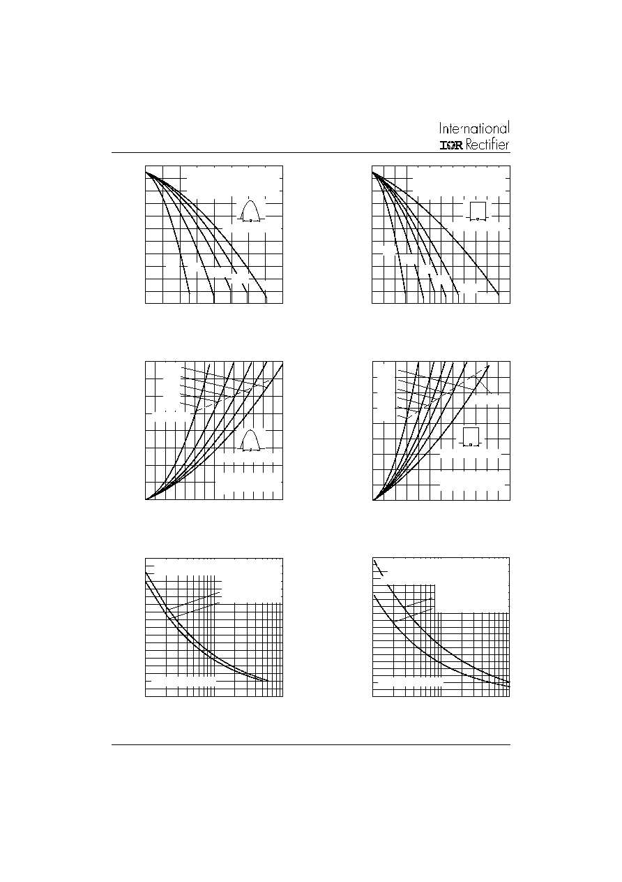
Fig. 1 - Current Ratings Characteristics
Fig. 2 - Current Ratings Characteristics
Outline Table
Case Style TO-200AC (B-PUK)
All dimensions in millimeters (inches)
TWO PLACES
PIN RECEPTACLE
AMP. 60598-1
0.7 (0.03) MIN.
34 (1.34) DIA. MAX.
53 (2.09) DIA. MAX.
5
8
.
5
(
2
.3
)
D
I
A
.
M
A
X
.
2 HOLES DIA. 3.5 (0.14) x
2.5 (0.1) DEEP
4.7 (0.18)
2
7
(
1
.
06)
M
A
X
.
0.7 (0.03) MIN.
6.2 (0.24) MIN.
20∞± 5∞
36.5 (1.44)
CREPAGE DISTANCE 36.33 (1.430) MIN.
STRIKE DISTANCE 17.43 (0.686) MIN.
Quote between upper and lower
pole pieces has to be considered
after application of Mounting Force
(see Thermal and Mechanical
Specification)
Average On-state Current (A)
Maximum Allowable Heatsink Temperature (
∞
C)
30
40
50
60
70
80
90
100
110
120
130
0
100
200
300
400
500
30∞
60∞
90∞
120∞
180∞
Conduction Angle
ST300C..L Series
(Single Side Cooled)
R (DC) = 0.11 K/W
thJ-hs
Average On-state Current (A)
Maximum Allowable Heatsink Temperature (∞C)
20
30
40
50
60
70
80
90
100
110
120
130
0
100 200 300 400 500 600 700
DC
30∞
60∞
90∞
120∞
180∞
Conduction Period
ST300C..L Series
(Single Side Cooled)
R (DC) = 0.11 K/W
thJ-hs
ST300C..L Series
6
www.irf.com
Bulletin I25193 rev. B 04/00
Fig. 3 - Current Ratings Characteristics
Fig. 4 - Current Ratings Characteristics
Fig. 5- On-state Power Loss Characteristics
Fig. 6- On-state Power Loss Characteristics
Fig. 7 - Maximum Non-Repetitive Surge Current
Single and Double Side Cooled
Fig. 8 - Maximum Non-Repetitive Surge Current
Single and Double Side Cooled
Maximum Allowable Heatsink Temperature (
∞
C)
Average On-state Current (A)
20
30
40
50
60
70
80
90
100
110
120
130
0
200
400
600
800
30∞
60∞
90∞
120∞
180∞
Conduction Angle
ST300C..L Series
(Double Side Cooled)
R (DC) = 0.05 K/W
thJ-hs
Average On-state Current (A)
Maximum Allowable Heatsink Temperature (
∞
C)
20
30
40
50
60
70
80
90
100
110
120
130
0
200
400
600
800 1000 1200
DC
30∞
60∞
90∞
120∞
180∞
Conduction Period
ST300C..L Series
(Double Side Cooled)
R (DC) = 0.05 K/W
thJ-hs
Maximum Average On-state Power Loss (W)
Average On-state Current (A)
0
200
400
600
800
1000
1200
1400
1600
0
100 200 300 400 500 600 700
180∞
120∞
90∞
60∞
30∞
RMS Limit
Conduction Angle
ST300C..L Series
T = 125∞C
J
Average On-state Current (A)
Maximum Average On-state Power Loss (W)
0
200
400
600
800
1000
1200
1400
1600
1800
0
200
400
600
800 1000 1200
DC
180∞
120∞
90∞
60∞
30∞
RMS Limit
Conduction Period
ST300C..L Series
T = 125∞C
J
3000
3500
4000
4500
5000
5500
6000
6500
7000
7500
1
10
100
ST300C..L Series
At Any Rated Load Condition And With
Rated Vrrm Applied Following Surge.
Initial Tj = 125∞C
@ 60 Hz 0.0083 s
@ 50 Hz 0.0100 s
3000
3500
4000
4500
5000
5500
6000
6500
7000
7500
8000
0.01
0.1
1
Versus Pulse Train Duration. Control
ST300C..L Series
Maximum Non Repetitive Surge Current
Of Conduction May Not Be Maintained.
Initial Tj = 125∞C
No Voltage Reapplied
Rated Vrrm Reapplied
Number Of Equal Amplitude Half Cycle Current Pulses (N)
Peak Half Sine Wave On-state Current (A)
Peak Half Sine Wave On-state Current (A)
Pulse Train Duration (s)
ST300C..L Series
7
www.irf.com
Bulletin I25193 rev. B 03/00
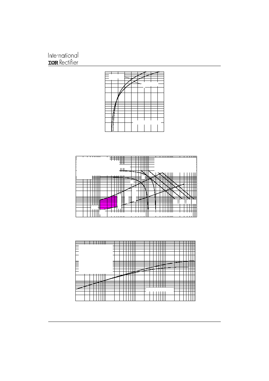
Fig. 9 - On-state Voltage Drop Characteristics
Fig. 10 - Thermal Impedance Z
thJ-hs
Characteristics
Fig. 11 - Gate Characteristics
100
1000
10000
0
1
2
3
4
5
6
7
8
9
T = 25∞C
J
T = 125∞C
J
ST300C..L Series
Instantaneous On-state Voltage (V)
Instantaneous On-state Current (A)
0.1
1
10
100
0.001
0.01
0.1
1
10
100
VGD
IGD
(b)
(a)
Tj
=
2
5
∞
C
Tj
=125
∞
C
Tj
=-
40
∞
C
(2) (3)
a) Recommended load line for
b) Recommended load line for
<=30% rated di/dt : 10V, 10ohms
Frequency Limited by PG(AV)
rated di/dt : 20V, 10ohms; tr<=1 µs
tr<=1 µs
(1)
(1) PGM = 10W, tp = 4ms
(2) PGM = 20W, tp = 2ms
(3) PGM = 40W, tp = 1ms
(4) PGM = 60W, tp = 0.66ms
Rectangular gate pulse
Device: ST300C..L Series
(4)
Square Wave Pulse Duration (s)
Transient Thermal Impedance Z
thJ-hs
(K/W)
0.001
0.01
0.1
1
0.001
0.01
0.1
1
10
Steady State Value
R = 0.11 K/W
(Single Side Cooled)
R = 0.05 K/W
(Double Side Cooled)
(DC Operation)
thJ-hs
thJ-hs
ST300C..L Series
Instantaneous Gate Current (A)
Instantaneous Gate Voltage (V)