
Features
Center amplifying gate
Metal case with ceramic insulator
International standard case TO-200AB (E-PUK)
Typical Applications
DC motor controls
Controlled DC power supplies
AC controllers
I
T(AV)
720
A
@ T
hs
55
∞C
I
T(RMS)
1420
A
@ T
hs
25
∞C
I
TSM
@
50Hz
9000
A
@ 60Hz
9420
A
I
2
t
@
50Hz
405
KA
2
s
@ 60Hz
370
KA
2
s
V
DRM
/V
RRM
400 to 1600
V
t
q
typical
100
µs
T
J
- 40 to 125
∞C
Parameters
ST330C..C
Units
Major Ratings and Characteristics
case style TO-200AB (E-PUK)
720A
PHASE CONTROL THYRISTORS
Hockey Puk Version
ST330C..C SERIES
1
Bulletin I25155 rev. D 04/03
www.irf.com

ST330C..C Series
2
Bulletin I25155 rev. D 04/03
www.irf.com
di/dt
Max. non-repetitive rate of rise
Gate drive 20V, 20
, t
r
1µs
of turned-on current
T
J
= T
J
max, anode voltage
80% V
DRM
Gate current 1A, di
g
/dt = 1A/µs
V
d
= 0.67% V
DRM
,
T
J
= 25∞C
I
TM
= 550A, T
J
= T
J
max, di/dt
= 40A/µs, V
R
= 50V
dv/dt
= 20V/µs, Gate 0V 100
,
t
p
= 500µs
Parameter
ST330C..C
Units Conditions
Switching
1000
A/µs
t
d
Typical delay time
1.0
t
q
Typical turn-off time
100
µs
Voltage
V
DRM
/V
RRM
, max. repetitive
V
RSM
, maximum non-
I
DRM
/I
RRM
max.
Type number
Code
peak and off-state voltage
repetitive peak voltage
@ T
J
= T
J
max
V
V
mA
04
400
500
08
800
900
ST330C..C
12
1200
1300
50
14
1400
1500
16
1600
1700
ELECTRICAL SPECIFICATIONS
Voltage Ratings
I
T(AV)
Max. average on-state current
720 (350)
A
180∞ conduction, half sine wave
@ Heatsink temperature
55 (75)
∞C
double side (single side) cooled
I
T(RMS)
Max. RMS on-state current
1420
DC @ 25∞C heatsink temperature double side cooled
I
TSM
Max. peak, one-cycle
9000
t = 10ms
No voltage
non-repetitive surge current
9420
A
t = 8.3ms
reapplied
7570
t = 10ms
100% V
RRM
7920
t = 8.3ms
reapplied
Sinusoidal half wave,
I
2
t
Maximum I
2
t for fusing
405
t = 10ms
No voltage
Initial T
J
= T
J
max.
370
t = 8.3ms
reapplied
287
t = 10ms
100% V
RRM
262
t = 8.3ms
reapplied
I
2
t
Maximum I
2
t for fusing
4050
KA
2
s
t = 0.1 to 10ms, no voltage reapplied
V
T(TO)
1
Low level value of threshold
voltage
V
T(TO)
2
High level value of threshold
voltage
r
t1
Low level value of on-state
slope resistance
r
t2
High level value of on-state
slope resistance
V
TM
Max. on-state voltage
1.96
V
I
pk
= 1810A, T
J
= T
J
max, t
p
= 10ms sine pulse
I
H
Maximum holding current
600
I
L
Typical latching current
1000
0.91
(16.7% x
x I
T(AV)
< I <
x I
T(AV)
), T
J
= T
J
max.
0.58
(16.7% x
x I
T(AV)
< I <
x I
T(AV)
), T
J
= T
J
max.
0.57
(I >
x I
T(AV)
),T
J
= T
J
max.
Parameter
ST330C..C
Units Conditions
0.92
(I >
x I
T(AV)
),T
J
= T
J
max.
On-state Conduction
KA
2
s
V
m
mA
T
J
= 25∞C, anode supply 12V resistive load
ST330C..C Series
3
Bulletin I25155 rev. D 04/03
www.irf.com
dv/dt
Maximum critical rate of rise of
off-state voltage
I
RRM
Max. peak reverse and off-state
I
DRM
leakage current
Blocking
500
V/
µ
s
T
J
= T
J
max. linear to 80% rated V
DRM
Parameter
ST330C..C
Units Conditions
50
mA
T
J
= T
J
max, rated V
DRM
/V
RRM
applied
P
GM
Maximum peak gate power
10.0
T
J
= T
J
max, t
p
5ms
P
G(AV)
Maximum average gate power
2.0
T
J
= T
J
max, f = 50Hz, d% = 50
I
GM
Max. peak positive gate current
3.0
A
T
J
= T
J
max, t
p
5ms
+V
GM
Maximum peak positive
gate voltage
-V
GM
Maximum peak negative
gate voltage
T
J
= - 40∞C
mA
T
J
= 25∞C
T
J
= 125∞C
T
J
= - 40∞C
V
T
J
= 25∞C
T
J
= 125∞C
I
GD
DC gate current not to trigger
10
mA
Parameter
ST330C..C
Units Conditions
20
5.0
Triggering
TYP.
MAX.
200
-
100
200
50
-
2.5
-
1.8
3.0
1.1
-
V
GD
DC gate voltage not to trigger
0.25
V
Max. gate current/voltage not to
trigger is the max. value which
will not trigger any unit with rated
V
DRM
anode-to-cathode applied
T
J
= T
J
max
Max. required gate trigger/ cur-
rent/ voltage are the lowest value
which will trigger all units 12V
anode-to-cathode applied
V
GT
DC gate voltage required
to trigger
I
GT
DC gate current required
to trigger
W
V
T
J
= T
J
max, t
p
5ms
T
J
Max. operating temperature range
-40 to 125
T
stg
Max. storage temperature range
-40 to 150
R
thJ-hs
Max. thermal resistance,
0.09
DC operation single side cooled
junction to heatsink
0.04
DC operation double side cooled
R
thC-hs
Max. thermal resistance,
0.02
DC operation single side cooled
case to heatsink
0.01
DC operation double side cooled
F
Mounting force, ± 10%
9800
N
(1000)
(Kg)
wt
Approximate weight
83
g
Parameter
ST330C..C
Units Conditions
K/W
Thermal and Mechanical Specification
∞C
Case style
TO - 200AB (E-PUK)
See Outline Table
K/W

ST330C..C Series
4
Bulletin I25155 rev. D 04/03
www.irf.com
1
-
Thyristor
2
-
Essential part number
3
-
0 = Converter grade
4
-
C = Ceramic Puk
5
-
Voltage code: Code x 100 = V
RRM
(See Voltage Rating Table)
6
-
C = Puk Case TO-200AB (E-PUK)
7
-
0 = Eyelet terminals (Gate and Auxiliary Cathode Unsoldered Leads)
1 = Fast-on terminals (Gate and Auxiliary Cathode Unsoldered Leads)
2 = Eyelet terminals (Gate and Auxiliary Cathode Soldered Leads)
3 = Fast-on terminals (Gate and Auxiliary Cathode Soldered Leads)
8
-
Critical dv/dt: None = 500V/µsec (Standard selection)
L
= 1000V/µsec (Special selection)
Ordering Information Table
R
thJ-hs
Conduction
(The following table shows the increment of thermal resistence R
thJ-hs
when devices operate at different conduction angles than DC)
Device Code
5
1
2
3
4
ST 33
0
C
16
C
1
7
6
8
Single Side Double Side Single Side Double Side
180∞
0.012
0.011
0.008
0.007
T
J
= T
J
max.
120∞
0.014
0.012
0.014
0.013
90∞
0.017
0.015
0.019
0.017
K/W
60∞
0.025
0.022
0.026
0.023
30∞
0.043
0.036
0.043
0.037
Sinusoidal conduction Rectangular conduction
Conduction angle
Units
Conditions

ST330C..C Series
5
Bulletin I25155 rev. D 04/03
www.irf.com
Outline Table
Case Style TO-200AB (E-PUK)
All dimensions in millimeters (inches)
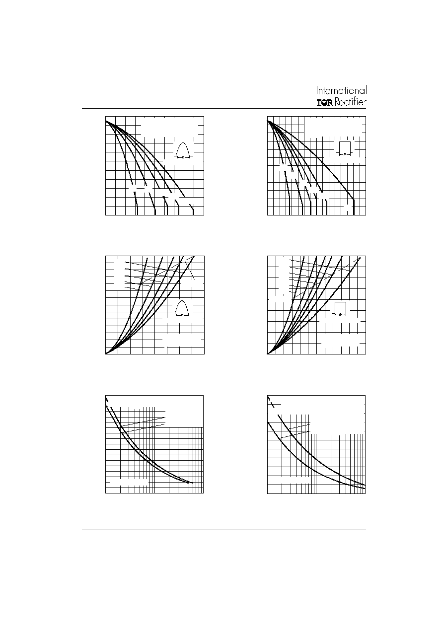
Fig. 1 - Current Ratings Characteristics
Fig. 2 - Current Ratings Characteristics
70
80
90
100
110
120
130
0
50 100 150 200 250 300 350 400
30∞
60∞
90∞
120∞
180∞
Average On-state Current (A)
Conduction Angle
M
a
x
i
m
u
m
A
l
l
o
w
a
bl
e H
e
ats
i
n
k
T
e
m
p
e
r
a
t
u
r
e
(
∞
C)
ST330C..C Series
(Single Side Cooled)
R (DC) = 0.09 K/ W
thJ-hs
20
30
40
50
60
70
80
90
100
110
120
130
0 100 200 300 400 500 600 700 800 900
DC
30∞
60∞
90∞
120∞ 180∞
Average On-state Current (A)
Conduction Period
M
a
x
i
m
u
m
A
l
l
o
w
abl
e
H
e
at
s
i
n
k
T
e
m
p
e
r
a
t
u
r
e
(
∞
C
)
ST330C..C Series
(Single Side Cooled)
R (DC) = 0.09 K/ W
thJ-hs
DIA. MAX.
4.75 (0.19)
28 (1.10)
6.5 (0.26)
0.3 (0.01) MIN.
0.3 (0.01) MIN.
ANODE TO GATE
CREEPAGE DISTANCE: 11.18 (0.44) MIN.
STRIKE DISTANCE: 7.62 (0.30) MIN.
25.3 (0.99)
14.1 / 15.1
(0.56 / 0.59)
25∞± 5∞
GATE TERM. FOR
1.47 (0.06) DIA.
PIN RECEPTACLE
25.3 (0.99)
40.5 (1.59) DIA. MAX.
DIA. MAX.
2 HOLES 3.56 (0.14) x
1.83 (0.07) MIN. DEEP
42 (1.65) MAX.
Quote between upper and lower
pole pieces has to be considered
after application of Mounting Force
(see Thermal and Mechanical
Specification)
ST330C..C Series
6
Bulletin I25155 rev. D 04/03
www.irf.com
Fig. 3 - Current Ratings Characteristics
Fig. 4 - Current Ratings Characteristics
Fig. 5- On-state Power Loss Characteristics
Fig. 6- On-state Power Loss Characteristics
Fig. 7 - Maximum Non-Repetitive Surge Current
Single and Double Side Cooled
10
20
30
40
50
60
70
80
90
100
110
120
130
0
200 400 600 800 1000 1200 1400 1600
DC
30∞
60∞
90∞
120∞
180∞
Average On-state Current (A)
Conduction Period
M
a
x
i
mu
m
A
l
l
o
w
a
b
l
e H
e
a
t
s
i
n
k
T
e
m
p
er
a
t
u
r
e (
∞
C
)
ST330C..C Series
(Double Side Cooled)
R (DC) = 0.04 K/ W
thJ-hs
20
30
40
50
60
70
80
90
100
110
120
130
0
200
400
600
800
1000
30∞
60∞
90∞
120∞
180∞
Average On-state Current (A)
Conduction Angle
M
a
x
i
m
u
m
A
l
l
o
w
a
bl
e
H
e
ats
i
n
k
T
e
m
p
e
r
atu
r
e
(
∞
C
)
ST330C..C Series
(Double Side Cooled)
R (DC) = 0.04 K/ W
thJ-hs
0
200
400
600
800
1000
1200
1400
1600
1800
0
200
400
600
800
1000 1200
DC
180∞
120∞
90∞
60∞
30∞
RMS Limit
Conduction Period
M
a
x
i
mu
m A
v
er
a
g
e
O
n
-
s
t
a
t
e
P
o
w
e
r
L
o
s
s
(W
)
Average On-state Current (A)
ST330C..C Series
T = 125∞C
J
0
200
400
600
800
1000
1200
1400
0
100 200 300 400 500 600 700 800
180∞
120∞
90∞
60∞
30∞
RMS Limit
Conduction Angle
M
a
x
i
mu
m A
v
e
r
a
g
e
O
n
-
s
ta
t
e
P
o
w
e
r
L
o
s
s
(
W
)
Average On-state Current (A)
ST330C..C Series
T = 125∞C
J
3500
4000
4500
5000
5500
6000
6500
7000
7500
8000
1
10
100
Number Of Equa l Amplitude Half Cycle Current Pulses (N)
Pe
a
k
H
a
l
f
S
i
n
e
W
a
v
e
O
n
-
s
t
a
te
C
u
r
r
e
n
t
(
A
)
Initial T = 125∞C
@ 60 Hz 0.0083 s
@ 50 Hz 0.0100 s
J
ST330C..C Series
At Any Rated Load Condition And With
Rated V Applied Following Surge.
RRM
3500
4000
4500
5000
5500
6000
6500
7000
7500
8000
8500
9000
0.01
0.1
1
Pulse Train Duration (s)
Versus Pulse Train Duration. Control
P
e
a
k
H
a
l
f
S
i
n
e
W
a
v
e
O
n
-
s
t
a
t
e
C
u
r
r
e
n
t
(
A
)
Initial T = 125∞C
No Voltage Reapplied
Rated V Reapplied
RRM
J
ST330C..C Series
Maximum Non Repetitive Surge Current
Of Conduction May Not Be Maintained.
Fig. 8 - Maximum Non-Repetitive Surge Current
Single and Double Side Cooled

ST330C..C Series
7
Bulletin I25155 rev. D 04/03
www.irf.com
Fig. 9 - On-state Voltage Drop Characteristics
Fig. 10 - Thermal Impedance Z
thJ-hs
Characteristics
Fig. 11 - Gate Characteristics
100
1000
10000
0
1
2
3
4
5
6
7
T = 25∞C
J
I
n
s
t
ant
an
e
o
u
s
O
n
-
s
t
a
t
e
C
u
r
r
e
n
t
(
A
)
Instantaneous On-state Voltage (V)
T = 125∞C
J
ST330C..C Series
0.001
0.01
0.1
0.001
0.01
0.1
1
10
Square Wave Pulse Duration (s)
th
J
-
h
s
Steady State Value
R = 0.09 K/ W
(Single Side Cooled)
R = 0.04 K/ W
(Double Side Cooled)
(DC Operation)
thJ-hs
thJ-hs
ST330C..C Series
T
r
a
n
s
i
en
t
T
h
er
m
a
l
I
m
p
e
d
a
n
c
e Z
(
K
/
W
)
0.1
1
10
100
0.001
0.01
0.1
1
10
100
VGD
IGD
(b)
(a)
Tj
=
2
5
∞
C
Tj
=
1
2
5
∞
C
Tj
=
-
4
0
∞
C
(2) (3)
Instantaneous Gate Current (A)
I
n
s
t
a
n
t
a
ne
ou
s
G
a
t
e
V
o
l
t
a
g
e
(
V
)
a) Recommended load line for
b) Recommended load line for
<=30% rated di/ dt : 10V, 10ohms
Frequency Limited by PG(AV)
rated di/ dt : 20V, 10ohms; tr<=1 µs
tr<=1 µs
(1)
(1) PGM = 10W, tp = 4ms
(2) PGM = 20W, tp = 2ms
(3) PGM = 40W, tp = 1ms
(4) PGM = 60W, tp = 0.66ms
Rectangular gate pulse
Device: ST330C..C Series
(4)

ST330C..C Series
8
Bulletin I25155 rev. D 04/03
www.irf.com
IR WORLD HEADQUARTERS: 233 Kansas St., El Segundo, California 90245, USA Tel: (310) 252-7105
TAC Fax: (310) 252-7309
Visit us at www.irf.com for sales contact information. 04 /03
Data and specifications subject to change without notice.
This product has been designed and qualified for Industrial Level.
Qualification Standards can be found on IR's Web site.