
720A
INVERTER GRADE THYRISTORS
Hockey Puk Version
ST333C..C SERIES
1
Bulletin I25170 rev. B 04/00
www.irf.com
case style TO-200AB (E-PUK)
Features
Metal case with ceramic insulator
International standard case TO-200AB (E-PUK)
All diffused design
Center amplifying gate
Guaranteed high dV/dt
Guaranteed high dI/dt
High surge current capability
Low thermal impedance
High speed performance
Typical Applications
Inverters
Choppers
Induction heating
All types of force-commutated converters
I
T(AV)
720
A
@ T
hs
55
∞C
I
T(RMS)
1435
A
@ T
hs
25
∞C
I
TSM
@
50Hz
11000
A
@ 60Hz
11500
A
I
2
t
@
50Hz
605
KA
2
s
@ 60Hz
553
KA
2
s
V
DRM
/V
RRM
400 to 800
V
t
q
range
10 to 30
µs
T
J
- 40 to 125
∞
C
Parameters
ST333C..C
Units
Major Ratings and Characteristics
ST333C..C Series
2
Bulletin I25170 rev. B 04/00
www.irf.com
Voltage
V
DRM
/V
RRM
, maximum
V
RSM
, maximum
I
DRM
/I
RRM
max.
Type number
Code
repetitive peak voltage
non-repetitive peak voltage
@ T
J
= T
J
max.
V
V
mA
04
400
500
08
800
900
ELECTRICAL SPECIFICATIONS
Voltage Ratings
Frequency
Units
50Hz
1630
1420
2520
2260
7610
6820
400Hz
1630
1390
2670
2330
4080
3600
1000Hz
1350
1090
2440
2120
2420
2100
A
2500Hz
720
550
1450
1220
1230
1027
Recovery voltage Vr
50
50
50
50
50
50
Voltage before turn-on Vd
V
DRM
V
DRM
V
DRM
Rise of on-state current di/dt
50
50
-
-
-
-
A/
µs
Heatsink temperature
40
55
40
55
40
55
∞C
Equivalent values for RC circuit
10
/ 0.47µF
10
/ 0.47µF
10
/ 0.47µF
I
TM
180
o
el
180
o
el
100
µs
I
TM
I
TM
Current Carrying Capability
V
I
T(AV)
Max. average on-state current
720 (350)
A
180∞ conduction, half sine wave
@ Heatsink temperature
55 (75)
∞C
double side (single side) cooled
I
T(RMS)
Max. RMS on-state current
1435
DC @ 25∞C heatsink temperature double side cooled
I
TSM
Max. peak, one half cycle,
11000
t = 10ms
No voltage
non-repetitive surge current
11500
A
t = 8.3ms
reapplied
9250
t = 10ms
100% V
RRM
9700
t = 8.3ms
reapplied
Sinusoidal half wave,
I
2
t
Maximum I
2
t for fusing
605
t = 10ms
No voltage
Initial T
J
= T
J
max
553
t = 8.3ms
reapplied
428
t = 10ms
100% V
RRM
391
t = 8.3ms
reapplied
I
2
t
Maximum I
2
t for fusing
6050
KA
2
s
t = 0.1 to 10ms, no voltage reapplied
Parameter
ST333C..C
Units
Conditions
On-state Conduction
KA
2
s
ST333C..C
50
ST333C..C Series
3
Bulletin I25170 rev. B 04/00
www.irf.com
V
TM
Max. peak on-state voltage
1.96
I
TM
= 1810A, T
J
= T
J
max, t
p
= 10ms sine wave pulse
V
T(TO)1
Low level value of threshold
voltage
V
T(TO)2
High level value of threshold
voltage
r
t
1
Low level value of forward
slope resistance
r
t
2
High level value of forward
slope resistance
I
H
Maximum holding current
600
T
J
= 25∞C, I
T
> 30A
I
L
Typical latching current
1000
T
J
= 25∞C, V
A
= 12V, Ra = 6
, I
G
= 1A
Parameter
ST333C..C
Units
Conditions
On-state Conduction
0.91
(16.7% x
x I
T(AV)
< I <
x I
T(AV)
), T
J
= T
J
max.
0.93
(I >
x I
T(AV)
), T
J
= T
J
max.
V
0.58
(16.7% x
x I
T(AV)
< I <
x I
T(AV)
), T
J
= T
J
max.
0.58
(I >
x I
T(AV)
), T
J
= T
J
max.
m
mA
di/dt
Max. non-repetitive rate of rise
T
J
= T
J
max, V
DRM
= rated V
DRM
of turned-on current
I
TM
= 2 x di/dt
T
J
= 25∞C, V
DM
= rated V
DRM
,
I
TM
= 50A DC, t
p
= 1µs
Resistive load, Gate pulse: 10V, 5
source
T
J
= T
J
max,
I
TM
= 550A, commutating di/dt
= 40A/µs
V
R
= 50V, t
p
= 500µs, dv/dt: see table in device code
Switching
Parameter
ST333C..C
Units
Conditions
1000
A/µs
t
d
Typical delay time
1.1
Min
Max
dv/dt
Maximum critical rate of rise of
T
J
= T
J
max. linear to 80% V
DRM
, higher value
off-state voltage
available on request
I
RRM
Max. peak reverse and off-state
I
DRM
leakage current
Parameter
ST333C..C
Units
Conditions
Blocking
500
V/
µs
50
mA
T
J
= T
J
max, rated V
DRM
/V
RRM
applied
P
GM
Maximum peak gate power
60
P
G(AV)
Maximum average gate power
10
I
GM
Max. peak positive gate current
10
A
T
J
= T
J
max, t
p
5ms
+V
GM
Maximum peak positive
gate voltage
-V
GM
Maximum peak negative
gate voltage
I
GT
Max. DC gate current required
to trigger
V
GT
Max. DC gate voltage required
to trigger
I
GD
Max. DC gate current not to trigger
20
mA
V
GD
Max. DC gate voltage not to trigger
0.25
V
Triggering
Parameter
ST333C..C
Units
Conditions
W
T
J
= T
J
max., f = 50Hz, d% = 50
20
5
V
T
J
= T
J
max, t
p
5ms
200
mA
3
V
T
J
= 25∞C, V
A
= 12V, Ra = 6
T
J
= T
J
max, rated V
DRM
applied
t
q
Max. turn-off time
10
30
µs
ST333C..C Series
4
Bulletin I25170 rev. B 04/00
www.irf.com
T
J
Max. operating temperature range
-40 to 125
T
stg
Max. storage temperature range
-40 to 150
R
thJ-hs
Max. thermal resistance,
0.09
DC operation single side cooled
junction to heatsink
0.04
DC operation double side cooled
R
thC-hs
Max. thermal resistance,
0.020
DC operation single side cooled
case to heatsink
0.010
DC operation double side cooled
F
Mounting force, ± 10%
9800
N
(1000)
(Kg)
wt
Approximate weight
83
g
Parameter
ST333C..C
Units
Conditions
K/W
Thermal and Mechanical Specification
∞C
Case style
TO - 200AB (E-PUK)
See Outline Table
K/W
R
thJ-hs
Conduction
(The following table shows the increment of thermal resistence R
thJ-hs
when devices operate at different conduction angles than DC)
Single Side Double Side
Single Side Double Side
180∞
0.010
0.011
0.007
0.007
120∞
0.012
0.012
0.012
0.013
90∞
0.015
0.015
0.016
0.017
K/W
T
J
= T
J
max.
60∞
0.022
0.022
0.023
0.023
30∞
0.036
0.036
0.036
0.036
Sinusoidal conduction
Rectangular conduction
Conduction angle
Units
Conditions
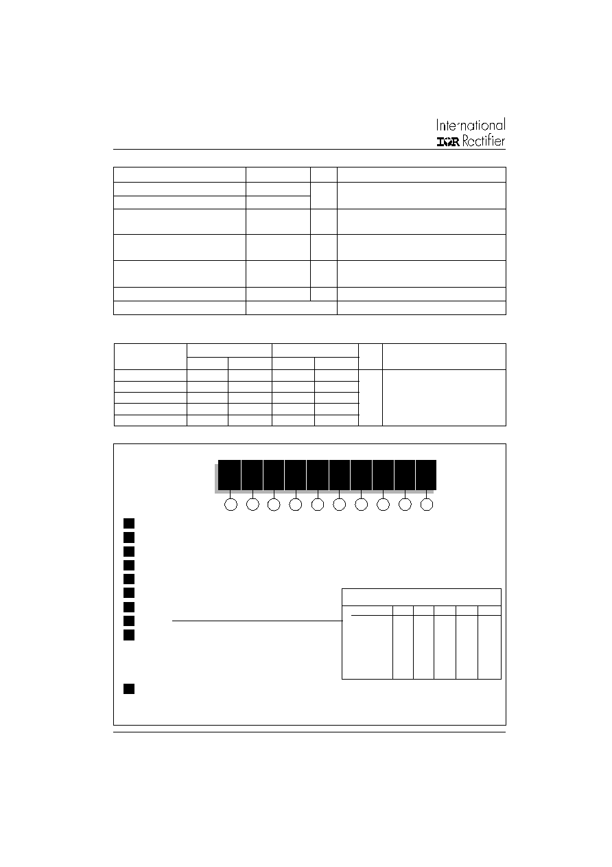
Ordering Information Table
ST
33
3
C
08
C
H
K
1
Device Code
5
6
8
9
3
4
10
7
1
2
1
- Thyristor
2
- Essential part number
3
- 3 = Fast turn off
4
- C = Ceramic Puk
5
- Voltage code: Code x 100 = V
RRM
(See Voltage Rating Table)
6
- C = Puk Case TO-200AB (E-PUK)
7
- Reapplied dv/dt code (for t
q
test condition)
8
- t
q
code
9
- 0 = Eyelet term. (Gate and Aux. Cathode Unsoldered Leads)
1 = Fast-on term. (Gate and Aux. Cathode Unsoldered Leads)
2 = Eyelet term. (Gate and Aux. Cathode Soldered Leads)
3 = Fast-on term. (Gate and Aux. Cathode Soldered Leads)
- Critical dv/dt:
None = 500V/µsec (Standard value)
L
= 1000V/µsec (Special selection)
dv/dt - t
q
combinations available
dv/dt (V/µs)
20
50
100
200
400
10
CN
DN
EN
--
--
12
CM
DM
EM
FM *
--
15
CL
DL
EL
FL *
HL
18
CP
DP
EP
FP
HP
20
CK
DK
EK
FK
HK
25
--
--
--
FJ
HJ
30
--
--
--
--
HH
t
q
(µs)
*
Standard part number.
All other types available only on request.
10
ST333C..C Series
5
Bulletin I25170 rev. B 04/00
www.irf.com
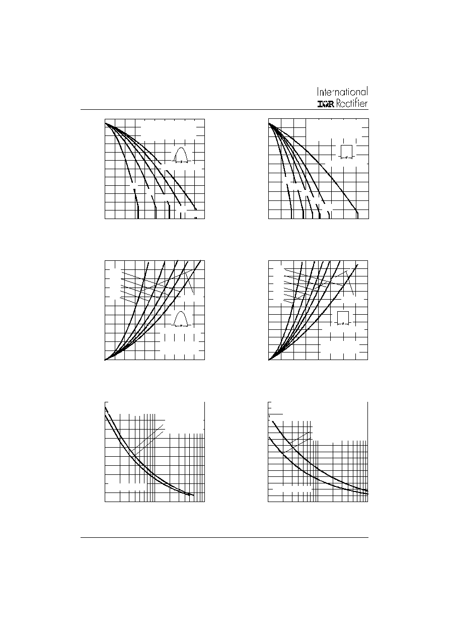
Fig. 1 - Current Ratings Characteristics
Fig. 2 - Current Ratings Characteristics
2 0
3 0
4 0
5 0
6 0
7 0
8 0
9 0
1 0 0
1 1 0
1 2 0
1 3 0
0
1 0 0 2 0 0 3 0 0 4 0 0 5 0 0 6 0 0 7 0 0 8 0 0 9 0 0
D C
3 0 ∞
6 0 ∞
9 0 ∞
1 2 0 ∞
1 8 0 ∞
A v e ra g e O n -st a te C u rre n t ( A )
Co nd uc tio n P e rio d
M
a
x
i
m
u
m
A
l
l
o
w
a
bl
e
He
at
s
i
n
k
T
e
m
p
e
r
at
u
r
e
(
∞
C
)
ST 3 3 3 C ..C S e rie s
( Sin g le S id e C o o le d )
R ( D C ) = 0 .0 9 K / W
th J -hs
2 0
3 0
4 0
5 0
6 0
7 0
8 0
9 0
1 0 0
1 1 0
1 2 0
1 3 0
0
10 0
20 0
30 0
4 0 0
5 0 0
60 0
30∞
60 ∞
9 0∞
1 20∞
180 ∞
Average On -state Current (A)
C o nd uc tio n A ng le
M
a
x
i
mum A
l
l
o
w
a
b
l
e
H
e
at
s
i
n
k
T
e
mp
e
r
at
ur
e
(
∞
C)
ST3 33C..C Series
(Single Side Cooled)
R (DC) = 0 .09 K/W
th J- hs
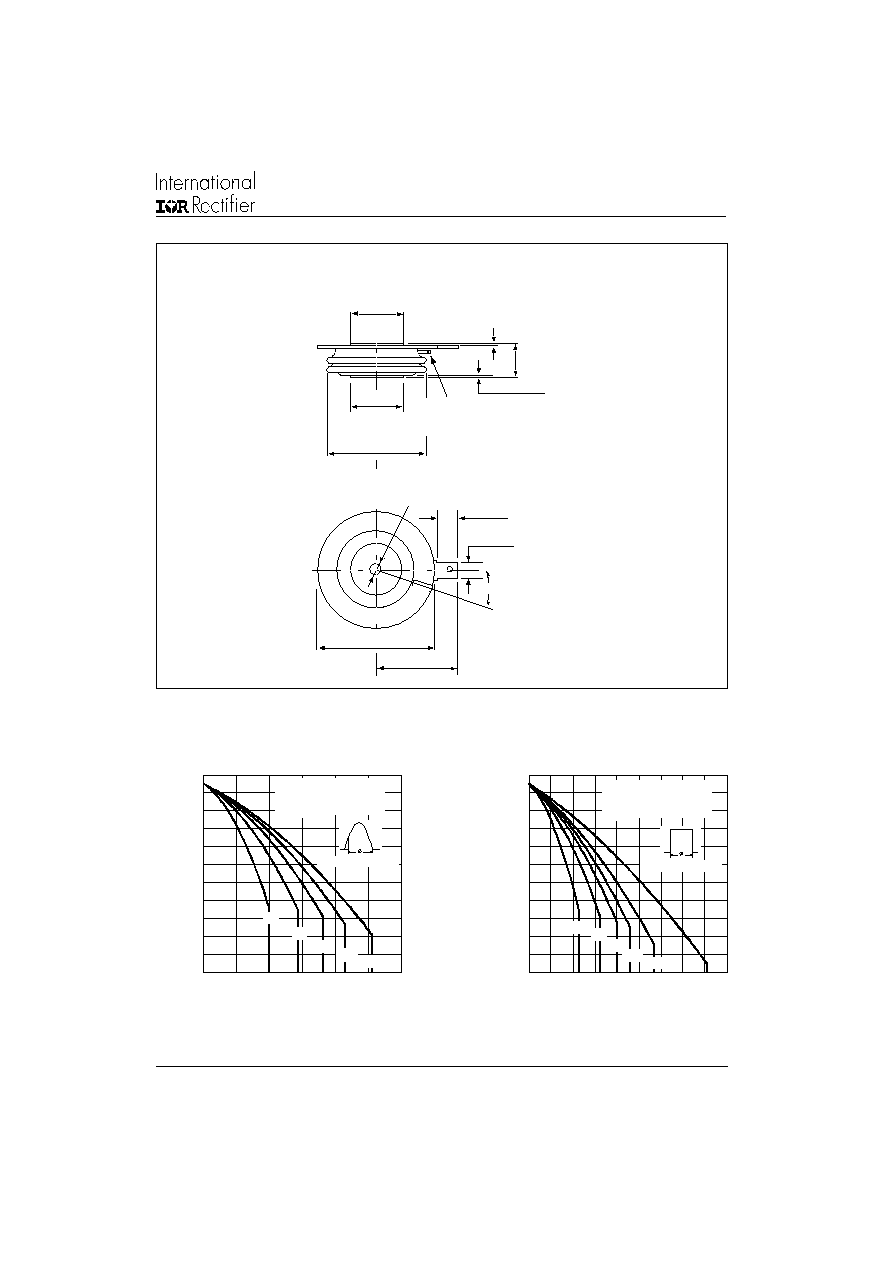
Outline Table
Case Style TO-200AB (E-PUK)
All dimensions in millimeters (inches)
DIA. MAX.
4.75 (0.19)
28 (1.10)
6.5 (0.26)
0.3 (0.01) MIN.
0.3 (0.01) MIN.
ANODE TO GATE
CREEPAGE DISTANCE: 11.18 (0.44) MIN.
STRIKE DISTANCE: 7.62 (0.30) MIN.
25.3 (0.99)
14.1 / 15.1
(0.56 / 0.59)
25∞± 5∞
GATE TERM. FOR
1.47 (0.06) DIA.
PIN RECEPTACLE
25.3 (0.99)
40.5 (1.59) DIA. MAX.
DIA. MAX.
2 HOLES 3.56 (0.14) x
1.83 (0.07) MIN. DEEP
42 (1.65) MAX.
Quote between upper and lower
pole pieces has to be considered
after application of Mounting Force
(see Thermal and Mechanical
Specification)
ST333C..C Series
6
Bulletin I25170 rev. B 04/00
www.irf.com
Fig. 3 - Current Ratings Characteristics
Fig. 4 - Current Ratings Characteristics
Fig. 5 - On-state Power Loss Characteristics
Fig. 6 - On-state Power Loss Characteristics
Fig. 7 - Maximum Non-repetitive Surge Current
Single and Double Side Cooled
Fig. 8 - Maximum Non-repetitive Surge Current
Single and Double Side Cooled
2 0
3 0
4 0
5 0
6 0
7 0
8 0
9 0
1 0 0
1 1 0
1 2 0
1 3 0
0
20 0 4 00 6 0 0 8 0 0 10 0 0 12 0 0 14 0 0 1 60 0
D C
30∞
60∞
90∞
1 20∞
180∞
Average O n-state Current (A)
C o nd u ctio n Pe riod
M
a
x
i
m
u
m A
l
l
o
w
a
bl
e
He
at
s
i
n
k
T
e
m
p
e
r
at
u
r
e
(
∞
C)
ST333C..C Series
( Double Side Cooled )
R (DC) = 0.04 K/W
th J -hs
1 0
2 0
3 0
4 0
5 0
6 0
7 0
8 0
9 0
1 0 0
1 1 0
1 2 0
1 3 0
0
2 0 0
4 0 0
6 0 0
8 0 0
1 0 0 0
3 0 ∞
6 0 ∞
9 0 ∞
1 2 0 ∞
1 8 0 ∞
A v e ra g e O n - st a t e C u rre n t ( A )
C o nd uctio n A ng le
M
a
x
i
m
u
m
A
l
l
o
w
a
b
l
e H
e
a
t
s
i
n
k
T
e
m
p
er
a
t
u
r
e (
∞
C)
ST 3 3 3 C ..C S e r ie s
( D o ub le Sid e C o o le d )
R ( D C ) = 0 .0 4 K /W
thJ -h s
0
2 0 0
4 0 0
6 0 0
8 0 0
1 0 0 0
1 2 0 0
1 4 0 0
1 6 0 0
1 8 0 0
2 0 0 0
2 2 0 0
2 4 0 0
2 6 0 0
0
2 0 0 4 0 0 6 0 0 8 0 0 1 0 0 0 1 2 0 0 1 4 0 0 1 6 0 0
D C
1 8 0 ∞
1 2 0 ∞
9 0 ∞
6 0 ∞
3 0 ∞
R M S L im it
C o nd u ctio n Pe rio d
M
a
x
i
m
u
m
Av
e
r
a
g
e
O
n
-
s
ta
te
P
o
w
e
r
L
o
s
s
(
W
)
A v e ra g e O n -st a t e C u rre n t ( A )
S T3 3 3 C ..C Se rie s
T = 1 2 5 ∞C
J
0
2 0 0
4 0 0
6 0 0
8 0 0
1 0 0 0
1 2 0 0
1 4 0 0
1 6 0 0
1 8 0 0
2 0 0 0
2 2 0 0
0
2 0 0
4 0 0
6 0 0
8 0 0
1 0 0 0
1 8 0 ∞
1 2 0 ∞
9 0 ∞
6 0 ∞
3 0 ∞
R M S L im it
C o nd u ctio n A ng le
M
a
x
i
mu
m
A
v
e
r
a
g
e
O
n
-
s
t
a
t
e
P
o
w
e
r
L
o
s
s
(
W
)
A v e ra g e O n -st a t e C u rre n t ( A )
ST 3 3 3 C ..C S e r ie s
T = 1 2 5 ∞C
J
4 0 0 0
5 0 0 0
6 0 0 0
7 0 0 0
8 0 0 0
9 0 0 0
1 0 0 0 0
1 1 0 0 0
1 2 0 0 0
0 .0 1
0 .1
1
Puls e T rain Duration (s)
Maxim um Non Repetitive Surge Current
V er sus Pulse Train Duration. C ontrol
O f Con duction May Not Be M ain tained.
Pe
a
k
H
a
l
f
S
i
n
e
W
a
v
e
O
n
-
s
ta
te
C
u
r
r
e
n
t
(
A
)
Initial T = 12 5∞C
No Voltage Reapplied
Rated V Reapplied
RR M
J
ST333C..C Series
4 5 00
5 0 00
5 5 00
6 0 00
6 5 00
7 0 00
7 5 00
8 0 00
8 5 00
9 0 00
9 5 00
1 00 0 0
1
1 0
1 0 0
N um b e r O f E q ua l A m p litud e H a lf C yc le C urrent Pulse s (N )
At An y Rated L oad Con dition And W ith
Rated V Applied Following Surge.
RR M
P
e
ak
Hal
f
S
i
n
e
W
a
v
e
O
n
-
s
t
a
t
e
C
u
r
r
e
n
t
(
A
)
In itial T = 125 ∞C
@ 6 0 Hz 0.008 3 s
@ 5 0 Hz 0.010 0 s
J
ST3 33C..C Series
ST333C..C Series
7
Bulletin I25170 rev. B 04/00
www.irf.com
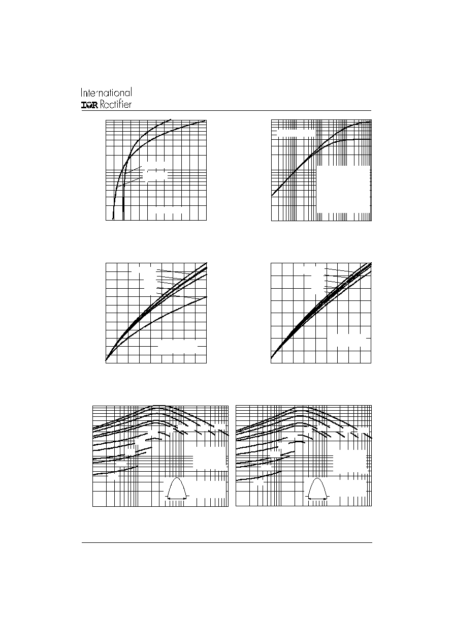
Fig. 9 - On-state Voltage Drop Characteristics
Fig. 10 - Thermal Impedance Z
thJ-hs
Characteristics
Fig. 11 - Reverse Recovered Charge Characteristics
Fig. 12 - Reverse Recovery Current Characteristics
Fig. 13 - Frequency Characteristics
1 00
10 0 0
1 0 00 0
0 .5 1 1 .5 2 2. 5 3 3. 5 4 4 .5 5 5 .5 6 6 .5
T = 25∞C
J
I
n
s
t
a
n
ta
n
e
o
u
s
O
n
-
s
ta
te
C
u
r
r
e
n
t
(
A
)
Instan tan eous O n-s tate V oltage (V)
T = 125 ∞C
J
ST3 33C..C Series
2 0
4 0
6 0
8 0
1 0 0
1 2 0
1 4 0
1 6 0
1 8 0
1 0
2 0
3 0
4 0
5 0
6 0
7 0
8 0
9 0 1 0 0
M
a
x
i
m
u
m
R
e
v
e
rs
e
R
e
c
o
v
e
ry
C
u
rre
n
t
-
I
rr
(
A
)
R a te O f Fa ll O f Fo rw a rd C ur re n t - d i/ d t ( A /µ s)
I = 5 00 A
3 00 A
20 0 A
1 00 A
50 A
T M
ST 3 3 3 C ..C S e rie s
T = 1 2 5 ∞ C
J
8 0
1 0 0
1 2 0
1 4 0
1 6 0
1 8 0
2 0 0
2 2 0
2 4 0
2 6 0
2 8 0
3 0 0
3 2 0
1 0
2 0
3 0
40
5 0
60
7 0
8 0
9 0 1 0 0
I = 50 0 A
3 00 A
2 00 A
10 0 A
50 A
Rate O f Fall O f O n-state Current - di/dt (A/µs)
M
a
x
i
m
u
m
R
e
ve
rse
R
e
c
o
ve
ry
C
h
a
r
g
e
-
Q
rr
(
µ
C
)
TM
ST333 C..C Series
T = 1 25 ∞C
J
0 .0 0 1
0 .0 1
0 .1
0 .0 0 1
0 .0 1
0 . 1
1
1 0
Sq u a re W a v e P u ls e D ur at io n ( s)
th
J
-
h
s
T
r
a
n
s
i
e
n
t
T
h
e
r
m
a
l
I
m
p
e
d
a
n
c
e
Z
(
K
/
W
)
S T3 3 3 C ..C Se r ie s
S te a d y St a t e V a lu e
R = 0 .0 9 K /W
( S in gle Sid e C o o le d )
R = 0 .0 4 K /W
( D o u b le S id e C o o le d )
( D C O p e ra t io n )
th J -hs
thJ -h s
1 E 1
1 E 2
1 E 3
1 E 4
5 0 H z
4 00
2 50 0
1 00
Pu lse B a se w id th ( µ s)
1 000
15 0 0
3 00 0
20 0
50 0
5 00 0
ST33 3C ..C Serie s
Sinuso id a l p ulse
T = 55∞C
C
Snub b er circ uit
R = 1 0 o hm s
C = 0.4 7 µF
V = 80 % V
s
s
D
D RM
t p
1 E 1
1 E 2
1 E 3
1 E 4
1 E 1
1 E 2
1 E 3
1 E 4
50 H z
4 00
25 00
1 00
P ulse B a se w id th ( µ s)
P
e
a
k
O
n
-
s
t
a
t
e
C
u
rre
n
t
(
A
)
1 000
1 50 0
3 00 0
20 0
50 0
50 00
ST33 3 C..C Serie s
Sin uso id a l p uls e
T = 40∞C
C
Snub b er c ircu it
R = 1 0 o hm s
C = 0 .47 µF
V = 80 % V
s
s
D
D RM
tp
1 E 4
ST333C..C Series
8
Bulletin I25170 rev. B 04/00
www.irf.com
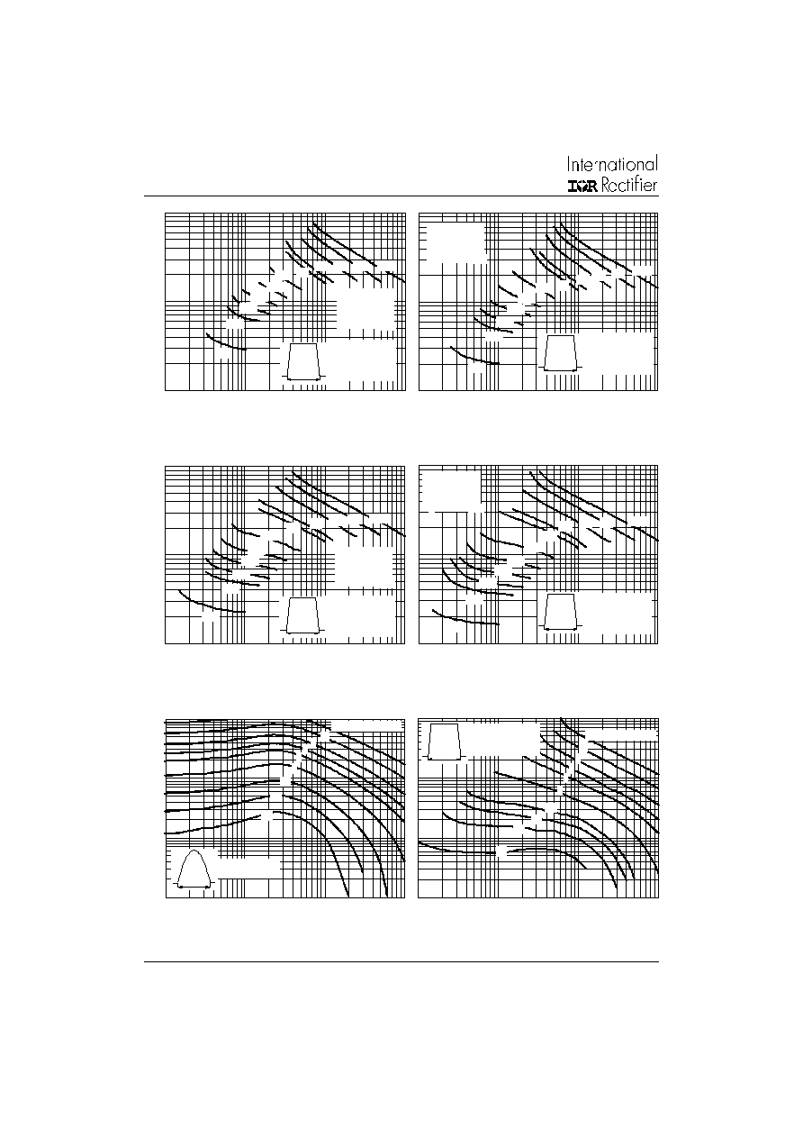
Fig. 14 - Frequency Characteristics
Fig. 15 - Frequency Characteristics
Fig. 16 - Maximum On-state Energy Power Loss Characteristics
1 E 2
1 E 3
1 E 4
1 E 1
1 E 2
1 E 3
1 E 4
5 0 H z
4 00
2 50 0
10 0
100 0
15 00
20 00
3 00 0
200
5 00
P u lse B ase w id t h ( µ s)
P
e
a
k
O
n
-
s
t
a
t
e
C
u
rre
n
t
(
A
)
ST33 3 C..C Serie s
Tra p e zoid a l p ulse
T = 40∞C
d i/d t = 100 A/µs
Snub b er c ircuit
R = 10 o hm s
C = 0 .47 µ F
V = 80 % V
s
s
D
D RM
C
50 00
tp
1 E 4
1 E 2
1 E 3
1 E 4
1 E 1
1 E 2
1 E 3
1 E 4
50 H z
40 0
2 5 00
10 0
100 0
15 00
20 0 0
2 00
50 0
P u lse Ba se w id t h ( µ s)
P
e
a
k
O
n
-
s
ta
te
C
u
r
r
e
n
t (
A
)
ST3 33 C.. C Se ries
Tra p ezo id a l p uls e
T = 4 0∞C
d i/d t = 50 A/µs
3 0 00
Snub b e r circuit
R = 1 0 o hm s
C = 0.47 µF
V = 80 % V
s
s
D
D RM
C
tp
5 00 0
1 E 4 1 E 1
1 E 2
1 E 3
1 E 4
50 H z
40 0
10 0
P u lse Ba se w id th ( µs)
10 00
1 5 00
20 00
2 00
50 0
2 50 0
Snub b e r circ uit
R = 1 0 o hm s
C = 0.4 7 µF
V = 80 % V
D RM
s
s
D
ST33 3C. .C Se ries
Tra p ezo id a l p uls e
T = 55 ∞C
d i/d t = 1 00A /µs
C
3 00 0
50 00
tp
1 E 1
1 E 1
1 E 2
1 E 3
1 E 4
5 0 H z
4 00
10 0
P u lse Ba se w id th ( µ s)
10 0 0
1 50 0
20 00
2 00
50 0
ST333 C.. C Se ries
Tra p ezo id a l p uls e
T = 55 ∞C
d i/d t = 10 0A /µs
C
2 50 0
Snub b e r circ uit
R = 1 0 o hm s
C = 0.4 7 µF
V = 80 % V
s
s
D
DR M
tp
3 00 0
5 00 0
1 E 1
1 E 1
1 E 2
1 E 3
1 E 4
1 E 1
1 E 2
1 E 3
1 E 4
P u lse B ase w id t h ( µ s)
20 jo ule s p e r p uls e
2
1
0.5
0 .3
0.2
10
5
P
e
a
k
O
n
-
s
t
a
t
e
C
u
rre
n
t
(
A
)
3
ST33 3C ..C Se ries
Sinuso id a l p uls e
tp
1 E 4 1 E 1
1 E 2
1 E 3
1 E 4
P u lse Ba se w id t h ( µ s)
2 0 jou les p er p ulse
2
1
0 .5
0.3
0.2
10
3
ST3 33 C Se ries
Rec ta ng ula r p uls e
d i/d t = 50A /µs
0.4
t p
5
1 E 1
ST333C..C Series
9
Bulletin I25170 rev. B 04/00
www.irf.com
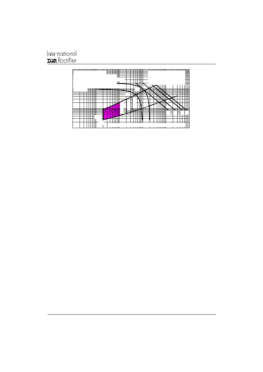
Fig. 17 - Gate Characteristics
0 . 1
1
1 0
1 0 0
0 . 0 0 1
0 . 0 1
0 . 1
1
1 0
1 0 0
V G D
IG D
( b )
( a )
Tj
=
2
5
∞
C
Tj
=
1
2
5
∞
C
T
j
=
-
40
∞
C
( 1 )
( 2 )
In sta n t a n e o u s G at e C u rr e n t ( A )
I
n
st
a
n
t
a
n
e
o
u
s G
a
t
e
V
o
l
t
a
g
e
(
V
)
Re c t a n g ula r g a t e p u lse
a ) R e c o m m e n d e d lo a d lin e fo r
b ) Re c o m m e n d e d lo a d lin e f o r
< = 3 0 % ra te d d i/d t : 1 0 V , 1 0 o h m s
ra t e d d i/d t : 2 0 V , 1 0 o h m s; t r< =1 µ s
t r< =1 µ s
( 1 ) P G M = 1 0 W , t p = 2 0 m s
( 2 ) P G M = 2 0 W , t p = 1 0 m s
( 3 ) P G M = 4 0 W , t p = 5 m s
( 4 ) P G M = 6 0 W , t p = 3 . 3 m s
(3 )
D e v ic e : ST 3 3 3 C .. C Se rie s Fre q u e n c y L im ite d b y P G (A V )
( 4 )