910A
PHASE CONTROL THYRISTORS
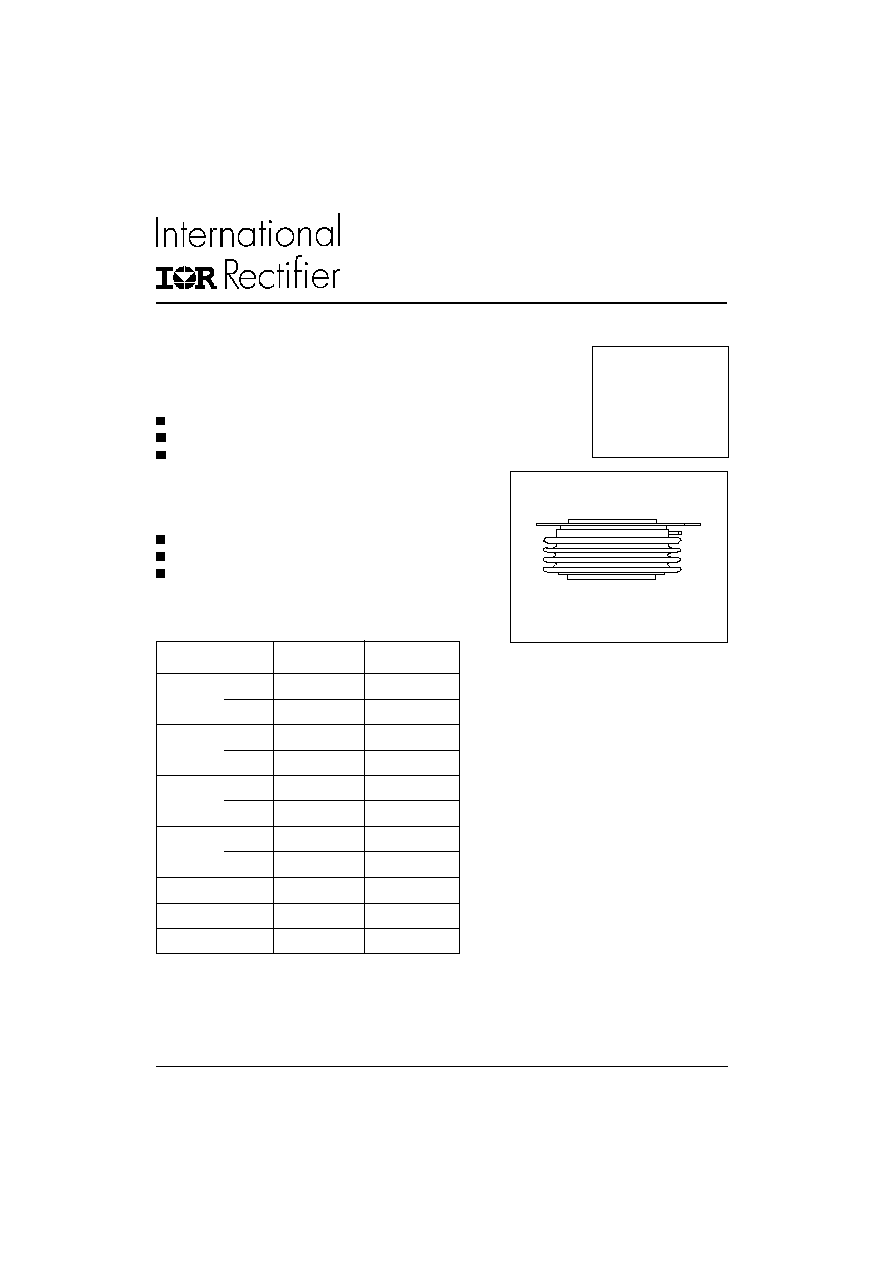
Hockey Puk Version
ST700C..L SERIES
1
Bulletin I25190 rev. D 04/00
www.irf.com
Features
Center amplifying gate
Metal case with ceramic insulator
International standard case TO-200AC (B-PUK)
Typical Applications
DC motor control
Controlled DC power supplies
AC controllers
I
T(AV)
910
A
@ T
hs
55
∞C
I
T(RMS)
1857
A
@ T
hs
25
∞C
I
TSM
@
50Hz
15700
A
@ 60Hz
16400
A
I
2
t
@
50Hz
1232
KA
2
s
@ 60Hz
1125
KA
2
s
V
DRM
/V
RRM
1200 to 2000
V
t
q
typical
150
µs
T
J
- 40 to 125
∞C
Parameters
ST700C..L
Units
Major Ratings and Characteristics
case style TO-200AC (B-PUK)
ST700C..L Series
2
www.irf.com
Bulletin I25190 rev. D 04/00
ELECTRICAL SPECIFICATIONS
Voltage Ratings
Voltage
V
DRM
/V
RRM
, max. repetitive
V
RSM
, maximum non-
I
DRM
/I
RRM
max.
Type number
Code
peak and off-state voltage
repetitive peak voltage
@ T
J
= T
J
max
V
V
mA
12
1200
1300
16
1600
1700
ST700C..L
18
1800
1900
80
20
2000
2100
I
T(AV)
Max. average on-state current
910 (355)
A
180∞ conduction, half sine wave
@ Heatsink temperature
55 (85)
∞C
double side (single side) cooled
I
T(RMS)
Max. RMS on-state current
1857
DC @ 25∞C heatsink temperature double side cooled
I
TSM
Max. peak, one-cycle
15700
t = 10ms
No voltage
non-repetitive surge current
16400
A
t = 8.3ms
reapplied
13200
t = 10ms
100% V
RRM
13800
t = 8.3ms
reapplied
Sinusoidal half wave,
I
2
t
Maximum I
2
t for fusing
1232
t = 10ms
No voltage
Initial T
J
= T
J
max.
1125
t = 8.3ms
reapplied
871
t = 10ms
100% V
RRM
795
t = 8.3ms
reapplied
I
2
t
Maximum I
2
t for fusing
12321
KA
2
s t = 0.1 to 10ms, no voltage reapplied
V
T(TO) 1
Low level value of threshold
voltage
V
T(TO) 2
High level value of threshold
voltage
r
t1
Low level value of on-state
slope resistance
r
t2
High level value of on-state
slope resistance
V
TM
Max. on-state voltage
1.80
V
I
pk
= 2000A, T
J
= T
J
max, t
p
= 10ms sine pulse
I
H
Maximum holding current
600
I
L
Typical latching current
1000
1.00
(16.7% x
x I
T(AV)
< I <
x I
T(AV)
), T
J
= T
J
max.
0.40
(16.7% x
x I
T(AV)
< I <
x I
T(AV)
), T
J
= T
J
max.
0.35
(I >
x I
T(AV)
),T
J
= T
J
max.
Parameter
ST700C..L
Units Conditions
1.13
(I >
x I
T(AV)
),T
J
= T
J
max.
On-state Conduction
KA
2
s
V
m
mA
T
J
= 25∞C, anode supply 12V resistive load
ST700C..L Series
3
www.irf.com
Bulletin I25190 rev. D 04/00
di/dt
Max. non-repetitive rate of rise
Gate drive 20V, 20
, t
r
1µs
of turned-on current
T
J
= T
J
max, anode voltage
80% V
DRM
Gate current 1A, di
g
/dt = 1A/µs
V
d
= 0.67% V
DRM
,
T
J
= 25∞C
I
TM
= 750A, T
J
= T
J
max, di/dt
= 60A/µs, V
R
= 50V
dv/dt
= 20V/µs, Gate 0V 100
, t
p
= 500µs
Parameter
ST700C..L
Units Conditions
Switching
1000
A/µs
t
d
Typical delay time
1.0
t
q
Typical turn-off time
150
µs
dv/dt
Maximum critical rate of rise of
off-state voltage
I
DRM
Max. peak reverse and off-state
I
RRM
leakage current
Blocking
500
V/
µs
T
J
= T
J
max. linear to 80% rated V
DRM
Parameter
ST700C..L
Units Conditions
80
mA
T
J
= T
J
max, rated V
DRM
/V
RRM
applied
P
GM
Maximum peak gate power
10.0
T
J
= T
J
max, t
p
5ms
P
G(AV)
Maximum average gate power
2.0
T
J
= T
J
max, f = 50Hz, d% = 50
I
GM
Max. peak positive gate current
3.0
A
T
J
= T
J
max, t
p
5ms
+V
GM
Maximum peak positive
gate voltage
-V
GM
Maximum peak negative
gate voltage
T
J
= - 40∞C
mA
T
J
= 25∞C
T
J
= 125∞C
T
J
= - 40∞C
V
T
J
= 25∞C
T
J
= 125∞C
I
GD
DC gate current not to trigger
10
mA
Parameter
ST700C..L
Units Conditions
20
5.0
Triggering
TYP.
MAX.
200
-
100
200
50
-
2.5
-
1.8
3.0
1.1
-
V
GD
DC gate voltage not to trigger
0.25
V
Max. gate current/voltage not to
trigger is the max. value which
will not trigger any unit with rated
V
DRM
anode-to-cathode applied
T
J
= T
J
max
Max. required gate trigger/ cur-
rent/ voltage are the lowest value
which will trigger all units 12V
anode-to-cathode applied
V
GT
DC gate voltage required
to trigger
I
GT
DC gate current required
to trigger
W
V
T
J
= T
J
max, t
p
5ms
ST700C..L Series
4
www.irf.com
Bulletin I25190 rev. D 04/00
T
J
Max. operating temperature range
-40 to 125
T
stg
Max. storage temperature range
-40 to 150
R
thJ-hs
Max. thermal resistance,
0.073
DC operation single side cooled
junction to heatsink
0.031
DC operation double side cooled
R
thC-hs
Max. thermal resistance,
0.011
DC operation single side cooled
case to heatsink
0.006
DC operation double side cooled
F
Mounting force, ± 10%
14700
N
(1500)
(Kg)
wt
Approximate weight
255
g
Parameter
ST700C..L
Units
Conditions
K/W
∞C
Case style
TO - 200AC (B-PUK)
See Outline Table
K/W
Thermal and Mechanical Specification
Single Side Double Side
Single Side Double Side
180∞
0.009
0.009
0.006
0.006
120∞
0.011
0.011
0.011
0.011
90∞
0.014
0.014
0.015
0.015
K/W
T
J
= T
J
max.
60∞
0.020
0.020
0.021
0.021
30∞
0.036
0.036
0.036
0.036
Sinusoidal conduction
Rectangular conduction
Conduction angle
Units
Conditions
R
thJ-hs
Conduction
(The following table shows the increment of thermal resistence R
thJ-hs
when devices operate at different conduction angles than DC)
1
-
Thyristor
2
-
Essential part number
3
-
0 = Converter grade
4
-
C = Ceramic Puk
5
-
Voltage code: Code x 100 = V
RRM
(See Voltage Rating Table)
6
-
L = Puk Case TO-200AC (B-PUK)
7
-
0 = Eyelet terminals (Gate and Auxiliary Cathode Unsoldered Leads)
1 = Fast-on terminals (Gate and Auxiliary Cathode Unsoldered Leads)
2 = Eyelet terminals (Gate and Auxiliary Cathode Soldered Leads)
3 = Fast-on terminals (Gate and Auxiliary Cathode Soldered Leads)
8
-
Critical dv/dt: None = 500V/µsec (Standard selection)
L
= 1000V/µsec (Special selection)
Ordering Information Table
Device Code
5
1
2
3
4
ST
70
0
C
20
L
1
7
6
8
ST700C..L Series
5
www.irf.com
Bulletin I25190 rev. D 04/00
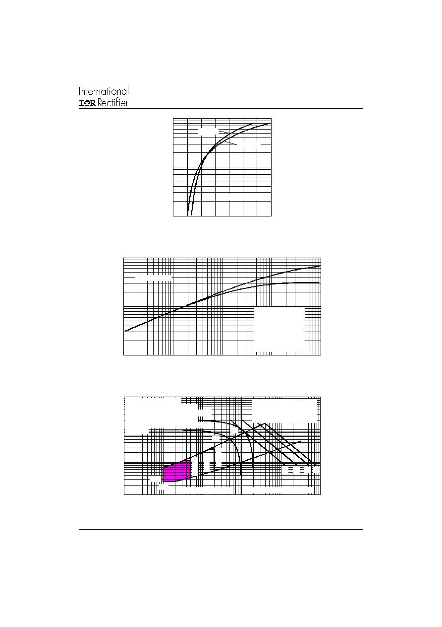
Fig. 1 - Current Ratings Characteristics
Fig. 2 - Current Ratings Characteristics
4 0
5 0
6 0
7 0
8 0
9 0
1 0 0
1 1 0
1 2 0
1 3 0
0
1 0 0
2 0 0
3 0 0
4 0 0
5 0 0
6 0 0
7 0 0
3 0 ∞
6 0 ∞
9 0 ∞
1 2 0 ∞
1 8 0 ∞
A v e r a g e O n -st a t e C u rre n t ( A )
C o nd uctio n A ng le
M
a
x
i
m
u
m A
l
l
o
w
a
b
l
e
H
e
a
t
s
i
n
k
T
e
mp
e
r
a
t
u
r
e
(
∞
C
)
S T 7 0 0 C ..L Se rie s
( S in gle S id e C o o le d )
R ( D C ) = 0 .0 7 3 K/ W
th J -hs
2 0
3 0
4 0
5 0
6 0
7 0
8 0
9 0
1 0 0
1 1 0
1 2 0
1 3 0
0
2 0 0
4 0 0
6 0 0
8 0 0
1 0 0 0
D C
3 0 ∞
6 0 ∞
9 0 ∞
1 2 0 ∞
1 8 0 ∞
A v e ra ge O n - sta t e C u rre n t ( A )
C on d uc tio n Pe rio d
M
a
xi
m
u
m
A
l
l
o
w
a
bl
e
He
at
s
i
n
k
T
e
m
p
e
r
at
u
r
e
(
∞
C)
ST 7 0 0 C ..L S e r ie s
( S in g le Sid e C o o le d )
R ( D C ) = 0 .0 7 3 K/ W
th J -hs
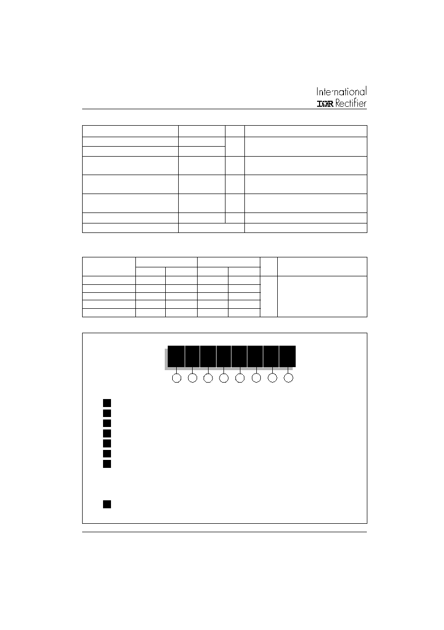
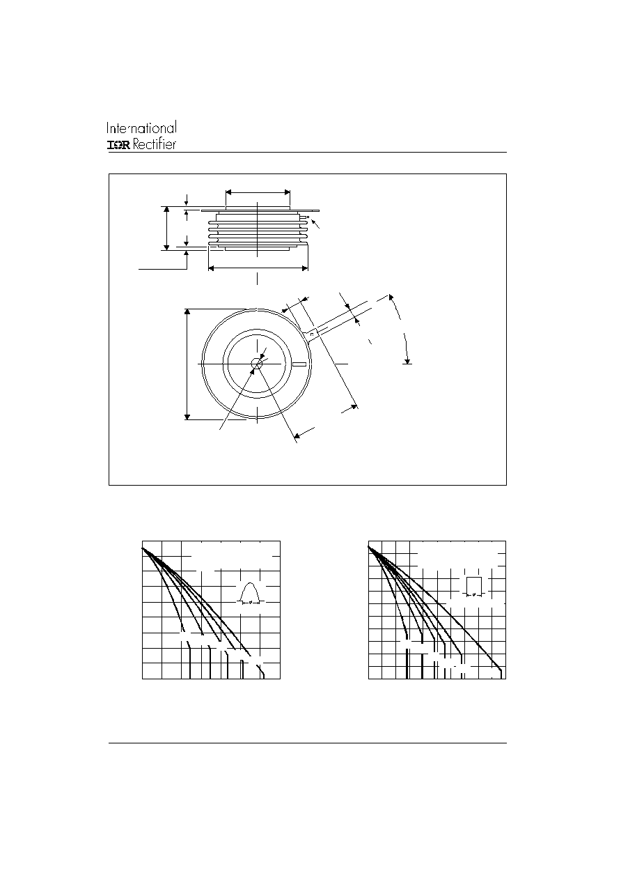
Outline Table
TWO PLACES
PIN RECEPTACLE
AMP. 60598-1
0.7 (0.03) MIN.
34 (1.34) DIA. MAX.
53 (2.09) DIA. MAX.
5
8
.5
(
2
.3
)
D
I
A
.
M
A
X
.
2 HOLES DIA. 3.5 (0.14) x
2.5 (0.1) DEEP
4.7 (0.18)
27
(
1
.
0
6)
M
A
X
.
0.7 (0.03) MIN.
6.2 (0.24) MIN.
20∞± 5∞
36.5 (1.44)
CREPAGE DISTANCE 36.33 (1.430) MIN.
STRIKE DISTANCE 17.43 (0.686) MIN.
Case Style TO-200AC (B-PUK)
All dimensions in millimeters (inches)
Quote between upper and lower
pole pieces has to be considered
after application of Mounting Force
(see Thermal and Mechanical
Specification)

ST700C..L Series
6
www.irf.com
Bulletin I25190 rev. D 04/00
Fig. 3 - Current Ratings Characteristics
Fig. 4 - Current Ratings Characteristics
Fig. 5- On-state Power Loss Characteristics
Fig. 6- On-state Power Loss Characteristics
Fig. 8 - Maximum Non-Repetitive Surge Current
Single and Double Side Cooled
Fig. 7 - Maximum Non-Repetitive Surge Current
Single and Double Side Cooled
2 0
3 0
4 0
5 0
6 0
7 0
8 0
9 0
1 0 0
1 1 0
1 2 0
1 3 0
0
4 0 0
8 0 0
1 2 0 0
1 6 0 0
2 0 0 0
D C
3 0 ∞
6 0 ∞
9 0 ∞
1 2 0 ∞
1 8 0 ∞
A v e r a g e O n -st a te C urre n t ( A )
C o nd u ctio n Pe rio d
M
a
x
i
m
u
m
A
l
l
o
w
a
bl
e
He
at
s
i
n
k
T
e
m
p
e
r
at
u
r
e
(
∞
C)
ST 7 0 0 C ..L Se rie s
( D o ub le S id e C o o le d )
R ( D C ) = 0 .0 3 1 K / W
thJ -hs
2 0
3 0
4 0
5 0
6 0
7 0
8 0
9 0
10 0
11 0
12 0
13 0
0
2 0 0
4 0 0
6 0 0
8 0 0
1 0 00
12 0 0
30 ∞
60 ∞
9 0∞
1 20∞
180 ∞
Average O n-sta te Current (A)
C o nd uc tio n A ng le
M
a
x
i
m
u
m A
l
l
o
w
a
bl
e
He
at
s
i
n
k
T
e
m
p
e
r
at
u
r
e
(
∞
C)
ST70 0C..L Series
(Double Side Cooled )
R (DC) = 0 .03 1 K/W
thJ - hs
0
4 00
8 00
1 20 0
1 60 0
2 00 0
2 40 0
2 80 0
0
2 00
40 0
60 0
80 0
1 0 00
12 0 0
180∞
120∞
90∞
60∞
30∞
RMS L im it
C o nd u ct io n A ng le
M
a
x
i
mu
m A
v
e
r
a
g
e
O
n
-
s
t
a
t
e
P
o
w
e
r
L
o
s
s
(
W
)
Av erage On -state Curren t (A)
ST7 00C..L Series
T = 1 25∞C
J
0
5 0 0
10 0 0
15 0 0
20 0 0
25 0 0
30 0 0
35 0 0
0
40 0
8 0 0
12 0 0
1 60 0
2 00 0
DC
180∞
120∞
90∞
60∞
30∞
RM S Lim it
C o nd uc tio n Pe rio d
Ma
x
i
m
u
m
A
v
e
r
a
g
e
O
n
-
s
ta
te
Po
w
e
r
L
o
s
s
(
W
)
Avera ge On -state Curren t (A)
ST70 0C..L Series
T = 12 5∞C
J
6 0 0 0
7 0 0 0
8 0 0 0
9 0 0 0
1 0 0 0 0
1 1 0 0 0
1 2 0 0 0
1 3 0 0 0
1 4 0 0 0
1
1 0
1 0 0
N um b er O f E q ua l A m p litud e H a lf C yc le C urren t Pulse s (N )
P
e
ak
Hal
f
S
i
n
e
W
a
v
e
O
n
-
s
t
a
t
e
C
u
r
r
e
n
t
(
A
)
In it ia l T = 1 2 5 ∞ C
@ 6 0 H z 0 .0 0 8 3 s
@ 5 0 H z 0 .0 1 0 0 s
J
S T 7 0 0 C ..L S e rie s
A t A n y R a t e d L o a d C o n d itio n A n d W it h
R a t e d V A p p lie d F o llo w in g Su rg e .
RRM
6 0 0 0
7 0 0 0
8 0 0 0
9 0 0 0
1 0 0 0 0
1 1 0 0 0
1 2 0 0 0
1 3 0 0 0
1 4 0 0 0
1 5 0 0 0
1 6 0 0 0
0 .0 1
0 .1
1
P u lse T ra in D u ra tio n ( s)
V e rsu s P ulse T ra in D u ra t io n . C o n t ro l
O f C o n d u c t io n M a y N o t Be M a in ta in e d .
P
e
ak
Ha
l
f
S
i
n
e
W
a
v
e
O
n
-
s
t
a
t
e
C
u
r
r
e
n
t
(
A
)
In it ia l T = 1 2 5 ∞ C
N o V o lta g e Re a p p lie d
Ra t e d V R e a p p lie d
RRM
J
ST 7 0 0 C ..L Se rie s
M a x im u m N o n R e p e t it iv e Su rg e C u rre n t
ST700C..L Series
7
www.irf.com
Bulletin I25190 rev. D 04/00
Fig. 9 - On-state Voltage Drop Characteristics
Fig. 10 - Thermal Impedance Z
thJ-hs
Characteristics
Fig. 11 - Gate Characteristics
1 0 0
1 0 0 0
1 0 0 0 0
0 . 5
1
1 . 5
2
2 . 5
3
3 . 5
4
T = 2 5 ∞ C
J
I
n
s
t
a
n
ta
n
e
o
u
s
O
n
-
s
ta
t
e
C
u
r
r
e
n
t (
A
)
In sta n t a n e o u s O n - st a te V o lt a g e ( V )
T = 1 2 5 ∞C
J
S T7 0 0 C . .L S e rie s
0 . 0 0 1
0 . 0 1
0 . 1
0 . 0 0 1
0 . 0 1
0 . 1
1
1 0
Sq u a re W a v e P ulse D ur at io n ( s)
th
J
-
h
s
St e a d y St a t e V a lu e
R = 0 .0 7 3 K / W
( Sin g le Sid e C o o le d )
R = 0 .0 3 1 K / W
( D o u ble Sid e C o o le d )
( D C O p e rat io n )
ST 7 0 0 C . .L Se rie s
thJ -hs
thJ -hs
T
r
a
n
s
i
e
n
t
T
h
e
r
m
a
l
I
m
pe
d
a
n
c
e
Z
(
K
/
W
)
0 . 1
1
1 0
1 0 0
0 . 0 0 1
0 . 0 1
0 . 1
1
1 0
1 0 0
V G D
IG D
( b )
( a )
Tj
=
2
5
∞
C
T
j
=
125
∞
C
Tj
=
-
4
0
∞
C
( 2 )
( 3 )
In sta n t a n e o u s G a te C u rre n t ( A )
I
n
st
a
n
t
a
n
e
o
u
s
G
a
t
e
V
o
l
t
a
g
e
(
V
)
a ) Re c o m m e n d e d lo a d lin e fo r
b ) Re c o m m e n d e d lo a d lin e f o r
< = 3 0 % ra t e d d i/ d t : 1 0 V , 1 0 o h m s
Fre q u e n c y L im ite d b y P G ( A V )
ra t e d d i/d t : 2 0 V , 1 0 o h m s; t r< =1 µ s
tr< = 1 µs
( 1 )
( 1 ) P G M = 1 0 W , t p = 4 m s
( 2 ) P G M = 2 0 W , t p = 2 m s
( 3 ) P G M = 4 0 W , t p = 1 m s
( 4 ) P G M = 6 0 W , t p = 0 . 6 6 m s
R e c t a n g ula r g a t e p ulse
D e v ic e : ST 7 0 0 C . . L S e rie s
( 4 )