ISD5100 ≠ SERIES
- 2 -
1. GENERAL DESCRIPTION
The ISD5100-Series ChipCorder
products provide high quality, fully integrated, single-chip
Record/Playback solutions for 2- to 16-minute messaging applications that are ideal for use in cellular
phones, automotive communications, GPS/navigation systems and other portable products. The
ISD5100-Series products are an enhancement of the ISD5000 architecture, providing: 1) the I
2
C serial
port - address, control and duration selection are accomplished through an I
2
C interface to minimize
pin count (ONLY two control lines required); 2) the capability of storing digital data, in addition to
analog, information. These features allow customers to store phone book numbers, system
configuration parameters and message address pointers for message management capability.
The ISD5100-Series includes:
∑ ISD5116 from 8 to 16 minutes
∑ ISD5108 from 4 to 8 minutes
∑ ISD5104 from 2 to 4 minutes
Analog functions and audio gating have also been integrated into the ISD5100-Series products to
allow easy interface with integrated digital cellular chip sets on the market. Audio paths have been
designed to enable full duplex conversation record, voice memo, answering machine (including
outgoing message playback) and call screening features. This product enables playback of messages
while the phone is in standby, AND both simplex and duplex playback of messages while on a phone
call.
Additional voice storage features for digital cellular phones include: 1) a personalized outgoing
message can be sent to the person by getting caller-ID information from the host chipset 2) a private
call announce while on call can be heard from the host by giving caller-ID on call waiting information
from the host chipset.
Logic Interface Options of 2.0V and 3.0V are supported by the ISD5100-Series to accommodate
portable communication products customers (2.0- and 3.0-volt required).
Like other ChipCorder
Æ
products, the ISD5100-Series integrate the sampling clock, anti-aliasing and
smoothing filters, and the multi-level storage array on a single-chip. For enhanced voice features, the
ISD5100-Series eliminate external circuitry by integrating automatic gain control (AGC), a power
amplifier/speaker driver, volume control, summing amplifiers, analog switches, and a car kit interface.
Input level adjustable amplifiers are also included, providing a flexible interface for multiple
applications.
Recordings are stored into on-chip nonvolatile memory cells, providing zero-power message storage.
This unique, single-chip solution is made possible through Winbond's patented multilevel storage
technology. Voice and audio signals are stored directly into solid-state memory in their natural,
uncompressed form, providing superior quality voice and music reproduction.

ISD5100 ≠ SERIES
Publication Release Date: March, 2003
- 3 -
Revision 0.1
2. FEATURES
Fully-Integrated Solution
∑ Single-chip voice record/playback solution
∑ Dual storage of digital and analog information
∑ Durations
8 to 16-minute duration (ISD5116)
4 to 8-minute duration (ISD5108)
2 to 4-minute duration (ISD5104)
Low Power Consumption
∑ +2.7 to +3.3V (V
CC
) Supply Voltage
∑ Supports 2.0V and 3.0V interface logic
∑ Operating Current:
I
CC Play
= 15 mA (typical)
I
CC Rec
= 30 mA (typical)
I
CC Feedthrough
= 12 mA (typical)
∑ Standby Current:
I
SB
= 1
µA (typical)
∑ Most stages can be individually powered down to minimize power consumption
Enhanced Voice Features
∑ One or two-way conversation record
∑ One or two-way message playback
∑ Voice memo record and playback
∑ Private call screening
∑ In-terminal answering machine
∑ Personalized outgoing message
∑ Private call announce while on call
Digital Memory Features
∑ Up to 4 Mb available (ISD5116)
∑ Up to 2 Mb available (ISD5108)
∑ Up to 1 Mb available (ISD5104)
∑ Storage of phone numbers, system configuration parameters and message address table in
cellular application
Easy-to-use and Control
∑ No compression algorithm development required
∑ User-controllable sampling rates
∑ Programmable analog interface
∑ Standard & Fast mode I
2
C serial interface (100kHz ≠ 400 kHz)
∑ Fully addressable to handle multiple messages
High Quality Solution
∑ High quality voice and music reproduction
∑ Winbond's standard 100-year message retention (typical)
∑ 100K record cycles (typical) for analog data
∑ 10K record cycles (typical) for digital data
Options
∑ Available in die form,TSOP and SOIC and PDIP (ISD5116 Only)
∑ Commercial (0 to +70∞C) and Industrial (-40 to +85∞C) available

ISD5100 ≠ SERIES
Publication Release Date: March, 2003
- 5 -
Revision 0.1
4. TABLE OF CONTENTS
1. GENERAL DESCRIPTION...................................................................................................................2
2. FEATURES ..........................................................................................................................................3
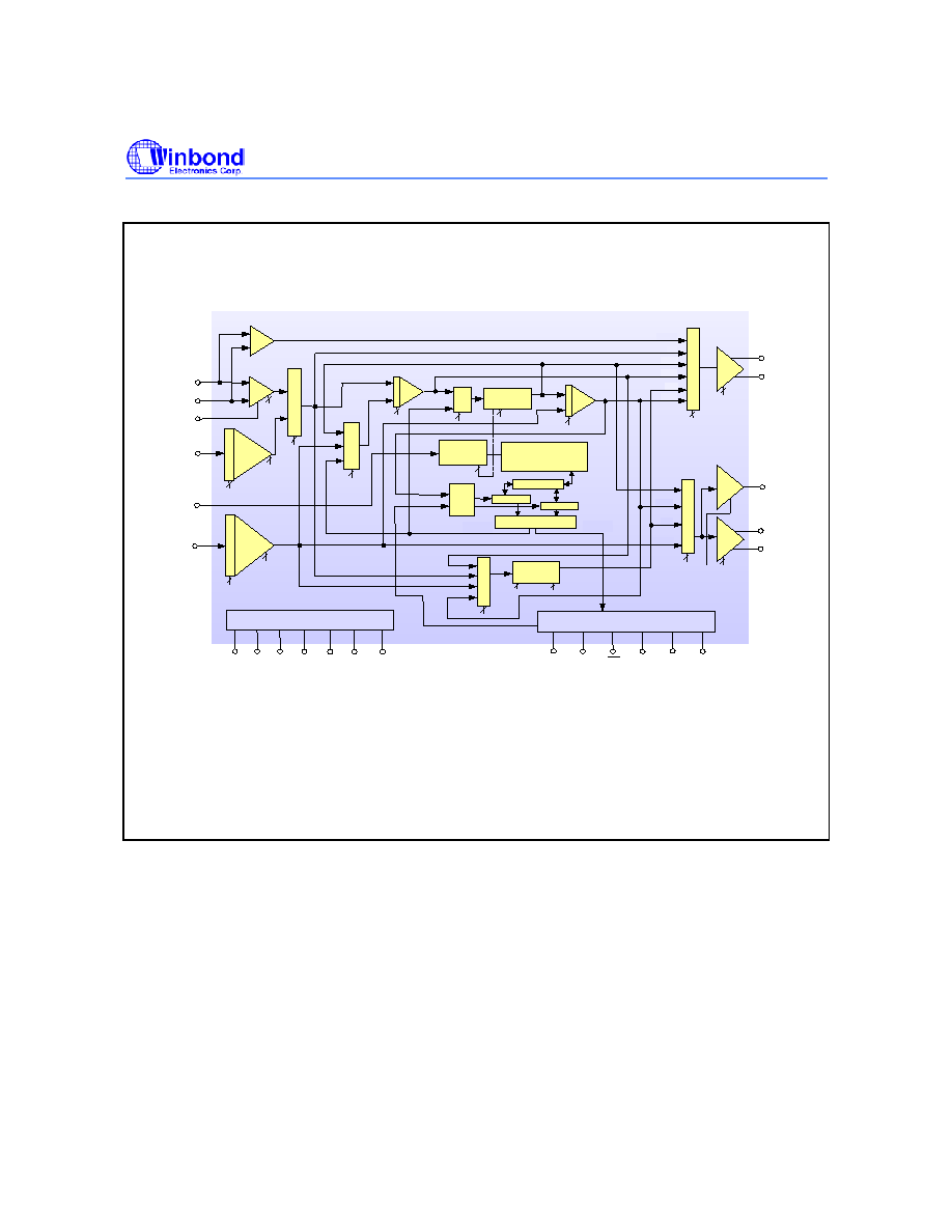
3. BLOCK DIAGRAM ...............................................................................................................................4
4. TABLE OF CONTENTS .......................................................................................................................5
5. PIN CONFIGURATION ........................................................................................................................7
6. PIN DESCRIPTION..............................................................................................................................8
7. FUNCTIONAL DESCRIPTION.............................................................................................................9
7.1. Overview ........................................................................................................................................9
7.1.1 Speech/Sound Quality .............................................................................................................9
7.1.2. Duration...................................................................................................................................9
7.1.3. Flash Technology....................................................................................................................9
7.1.4. Microcontroller Interface .......................................................................................................10
7.1.5. Programming.........................................................................................................................10
7.2. Functional Details ........................................................................................................................10
7.2.1. Internal Registers ..................................................................................................................11
7.2.2. Memory Architecture .............................................................................................................11
7.3. Operational Modes Description ...................................................................................................12
7.3.1. I
2
C Interface ..........................................................................................................................12
7.3.2. I
2
C Control Registers ............................................................................................................16
7.3.3. Opcode Summary .................................................................................................................17
7.3.4. Data Bytes.............................................................................................................................19
7.3.5. Configuration Resiter Bytes ..................................................................................................20
7.3.6. Power-up Sequence..............................................................................................................21
7.3.7. Feed Through Mode..............................................................................................................22
7.3.8. Call Record ...........................................................................................................................24
7.3.9. Memo Record........................................................................................................................25
7.3.10. Memo and Call Playback ....................................................................................................26
7.3.11. Message Cueing .................................................................................................................27
7.4. Analog Mode................................................................................................................................28
7.4.1. Aux In and Ana In Description ..............................................................................................28
7.4.2. ISD5100-Series Analog Structure (left half) Description ......................................................30
7.4.3. ISD5100-Series Aanalog Structure (right half) Description ..................................................31
7.4.4. Volume Control Description ..................................................................................................32
7.4.5. Speaker and Aux Out Description.........................................................................................33