ISD2532/40/48/64
SINGLE-CHIP, MULTIPLE-MESSAGES,
VOICE RECORD/PLAYBACK DEVICE
32-, 40-, 48-, AND 64-SECOND DURATION
Publication Release Date: June 2003
- 1 -
Revision 1.0

ISD2532/40/48/64
1. GENERAL DESCRIPTION
Winbond's ISD2500 ChipCorder
Æ
Series provide high-quality, single-chip, Record/Playback solutions
for 32- to 64-second messaging applications. The CMOS devices include an on-chip oscillator,
microphone preamplifier, automatic gain control, antialiasing filter, smoothing filter, speaker amplifier,
and high density multi-level storage array. In addition, the ISD2500 is microcontroller compatible,
allowing complex messaging and addressing to be achieved. Recordings are stored into on-chip
nonvolatile memory cells, providing zero-power message storage. This unique, single-chip solution is
made possible through Winbond's patented multilevel storage technology. Voice and audio signals
are stored directly into memory in their natural form, providing high-quality, solid-state voice
reproduction.
2. FEATURES
∑
Single 5 volt power supply
∑
Single-chip with duration of 32, 40, 48, or 64 seconds.
∑
Easy-to-use single-chip, voice record/playback solution
∑
High-quality, natural voice/audio reproduction
∑
Manual switch or microcontroller compatible
∑
Playback can be edge- or level-activated
∑
Directly cascadable for longer durations
∑
Automatic power-down (push-button mode)
- Standby current 1 µA (typical)
∑
Zero-power message storage
- Eliminates battery backup circuits
∑
Fully addressable to handle multiple messages
∑
100-year message retention (typical)
∑
100,000 record cycles (typical)
∑
On-chip clock source
∑
Programmer support for play-only applications
∑
Available in die form, PDIP, SOIC and TSOP packaging
∑
Temperature options: die (0
∞C to +50∞C) and package (0∞C to +70∞C)
- 2 -

ISD2532/40/48/64
4. TABLE OF CONTENTS
1. GENERAL DESCRIPTION.................................................................................................................. 2
2. FEATURES ......................................................................................................................................... 2
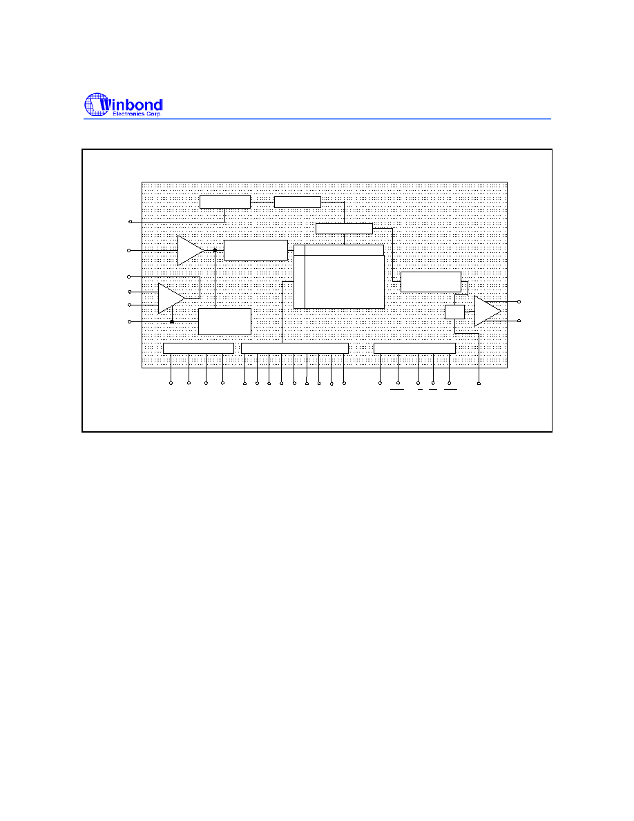
3. BLOCK DIAGRAM .............................................................................................................................. 3
4. TABLE OF CONTENTS ...................................................................................................................... 4
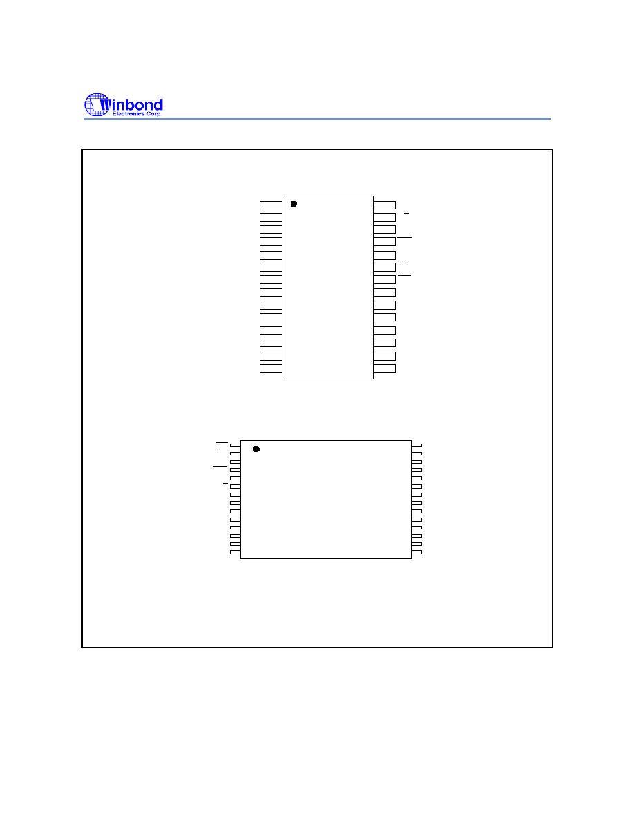
5. PIN CONFIGURATION ....................................................................................................................... 5
6. PIN DESCRIPTION............................................................................................................................. 6
7. FUNCTIONAL DESCRIPTION.......................................................................................................... 10
7.1. Detailed Description.................................................................................................................... 10
7.2. Operational Modes ..................................................................................................................... 11
7.2.1. Operational Modes Description............................................................................................ 12
8. TIMING DIAGRAMS.......................................................................................................................... 16
9. ABSOLUTE MAXIMUM RATINGS.................................................................................................... 19
9.1 Operating Conditions ................................................................................................................... 20
10. ELECTRICAL CHARACTERISTICS ............................................................................................... 21
10.1. Parameters For Packaged Parts .............................................................................................. 21
10.1.1. Typical Parameter Variation with Voltage and Temperature - Packaged Parts ................ 24
10.2. Parameters For Die .................................................................................................................. 25
10.2.1. Typical Parameter Variation with Voltage and Temperature - Die .................................... 28
10.3. Parameters For Push-Button Mode.......................................................................................... 29
11. TYPICAL APPLICATION CIRCUIT................................................................................................. 30
12. PACKAGE DRAWING AND DIMENSIONS .................................................................................... 35
12.1. 28-Lead 300-Mil Plastic Small Outline IC (SOIC)..................................................................... 35
12.2. 28-Lead 600-Mil Plastic Dual Inline Package (PDIP)............................................................... 36
12.3. 28-Lead 8x13.4mm Plastic Thin Small Outline Package (TSOP) Type 1................................ 37
12.4. Die Bonding Physical Layout
[1]
................................................................................................ 38
14. VERSION HISTORY ....................................................................................................................... 41
- 4 -