
ISD/Winbond ∑ 2727 North First Street, San Jose, CA 95134 ∑ TEL: 408/943-6666 ∑ FAX: 408/544-1787 ∑ http://www.isd.com
August 2000
Figure: ISD4004 Series Block Diagram
GENERAL DESCRIPTION
The ISD4004 ChipCorder
Æ
Products provide high-
quality, 3-volt, single-chip record/playback solu-
tions for 8- to 16-minute messaging applications
which are ideal for cellular phones and other por-
table products. The CMOS-based devices include
an on-chip oscillator, antialiasing filter, smoothing
filter, AutoMuteTM feature, audio amplifier, and
high density, multilevel Flash storage array. The
ISD4004 series is designed to be used in a micro-
processor- or microcontroller-based system. Ad-
dress and control are accomplished through a
Serial Peripheral Interface (SPI) or Microwire Serial
Interface to minimize pin count.
Recordings are stored in on-chip nonvolatile
memory cells, providing zero-power message
storage. This unique, single-chip solution is made
possible through ISD's patented multilevel storage
technology. Voice and audio signals are stored
directly into memory in their natural form, providing
high-quality, solid-state voice reproduction.
ISD4004 Series
Single-Chip Voice Record/Playback Devices
8-, 10-, 12-, and 16-Minute Durations
ISD4004 Series
ii
Voice Solutions in Silicon
TM
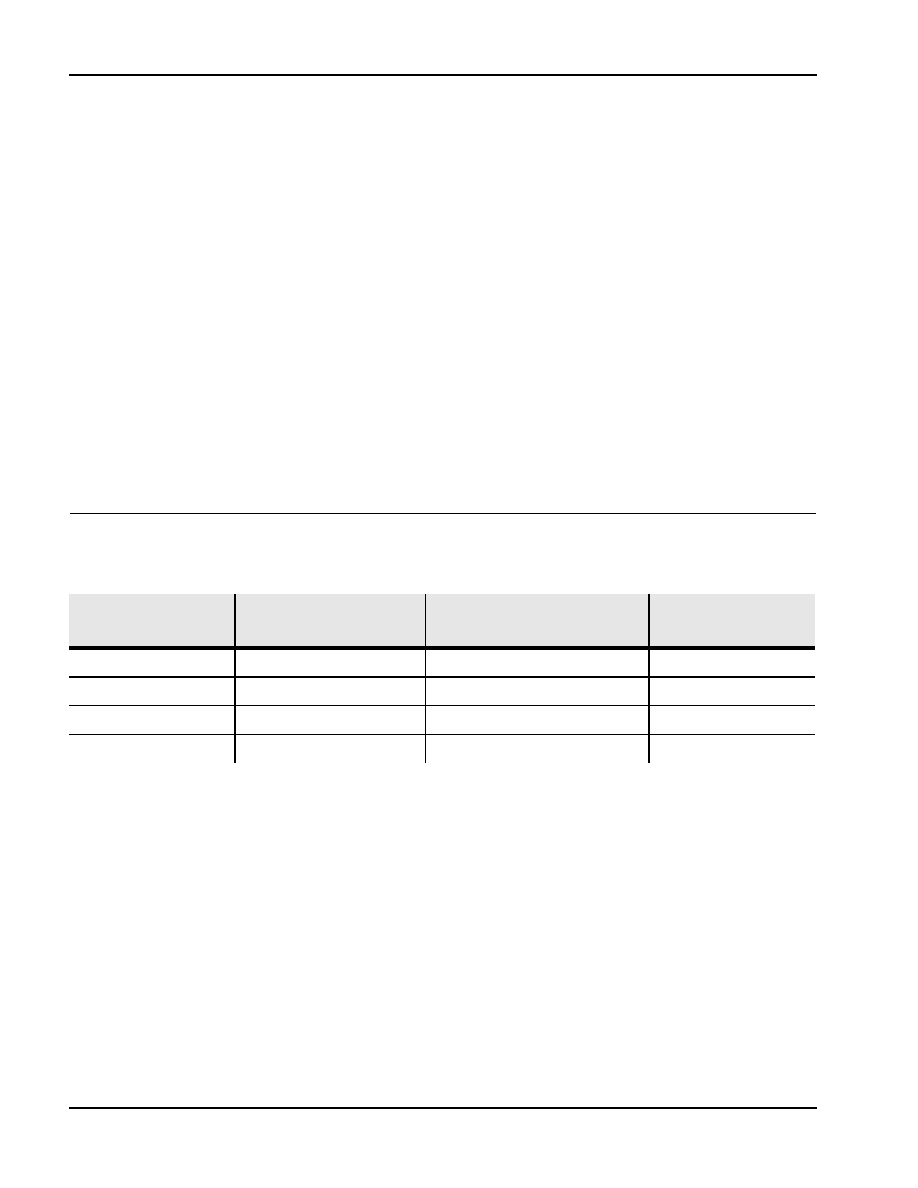
Table: ISD4004 Series Summary
Part
Number
Duration
(minutes)
Input Sample
Rate (KHz)
Typical Filter Pass
Band (KHz)
ISD4004-08M
8.0
8.0
3.4
ISD4004-10M
10.0
6.4
2.7
ISD4004-12M
12.0
5.3
2.3
ISD4004-16M
16.0
4.0
1.7
FEATURES
∑
Single-chip voice record/playback solution
∑
Single +3 volt supply
∑
Low-power consumption
≠ Operating current:
I
CC
Play = 15 mA (typical)
I
CC
Rec = 25 mA (typical)
≠ Standby current: 1 µA (typical)
∑
Single-chip durations of 8, 10, 12, and
16 minutes
∑
High-quality, natural voice/audio reproduction
∑
AutoMute feature provides background noise
attenuation during periods of silence
∑
No algorithm development required
∑
Microcontroller SPI or MicrowireTM Serial
Interface
∑
Fully addressable to handle multiple
messages
∑
Nonvolatile message storage
∑
Power consumption controlled by SPI
or Microwire control register
∑
100-year message retention (typical)
∑
100K record cycles (typical)
∑
On-chip clock source
∑
Available in die form, PDIP, SOIC, and TSOP
∑
Extended temperature (≠20∞C to +70∞C) and
industrial temperature (≠40∞C to +85∞C)
versions available

Table of Contents
ISD
iii
DETAILED DESCRIPTION . . . . . . . . . . . . . . . . . . . . . . . . . . . . . . . . . . . . . . . . . . . . . . . . . . . . . . . . . . . . . . . 1
Speech/Sound Quality . . . . . . . . . . . . . . . . . . . . . . . . . . . . . . . . . . . . . . . . . . . . . . . . . . . . . . . . . . . . 1
Duration . . . . . . . . . . . . . . . . . . . . . . . . . . . . . . . . . . . . . . . . . . . . . . . . . . . . . . . . . . . . . . . . . . . . . . . 1
Flash Storage . . . . . . . . . . . . . . . . . . . . . . . . . . . . . . . . . . . . . . . . . . . . . . . . . . . . . . . . . . . . . . . . . . . 1
Microcontroller Interface . . . . . . . . . . . . . . . . . . . . . . . . . . . . . . . . . . . . . . . . . . . . . . . . . . . . . . . . . . 1
Programming . . . . . . . . . . . . . . . . . . . . . . . . . . . . . . . . . . . . . . . . . . . . . . . . . . . . . . . . . . . . . . . . . . . 1
PIN DESCRIPTIONS . . . . . . . . . . . . . . . . . . . . . . . . . . . . . . . . . . . . . . . . . . . . . . . . . . . . . . . . . . . . . . . . . . . 1
Voltage Inputs (V
CCA
, V
CCD
) . . . . . . . . . . . . . . . . . . . . . . . . . . . . . . . . . . . . . . . . . . . . . . . . . . . . . . . 1
Ground Inputs (V
SSA
, V
SSD
) . . . . . . . . . . . . . . . . . . . . . . . . . . . . . . . . . . . . . . . . . . . . . . . . . . . . . . . . . 1
Non-Inverting Analog Input (ANA IN+) . . . . . . . . . . . . . . . . . . . . . . . . . . . . . . . . . . . . . . . . . . . . . . . . 3
Inverting Analog Input (ANA IN≠) . . . . . . . . . . . . . . . . . . . . . . . . . . . . . . . . . . . . . . . . . . . . . . . . . . . . 3
Audio Output (AUD OUT) . . . . . . . . . . . . . . . . . . . . . . . . . . . . . . . . . . . . . . . . . . . . . . . . . . . . . . . . . . 3
Slave Select (SS) . . . . . . . . . . . . . . . . . . . . . . . . . . . . . . . . . . . . . . . . . . . . . . . . . . . . . . . . . . . . . . . . . 3
Master Out Slave In (MOSI) . . . . . . . . . . . . . . . . . . . . . . . . . . . . . . . . . . . . . . . . . . . . . . . . . . . . . . . . . 3
Master In Slave Out (MISO) . . . . . . . . . . . . . . . . . . . . . . . . . . . . . . . . . . . . . . . . . . . . . . . . . . . . . . . . . 3
Serial Clock (SCLK) . . . . . . . . . . . . . . . . . . . . . . . . . . . . . . . . . . . . . . . . . . . . . . . . . . . . . . . . . . . . . . . 3
Interrupt (INT) . . . . . . . . . . . . . . . . . . . . . . . . . . . . . . . . . . . . . . . . . . . . . . . . . . . . . . . . . . . . . . . . . . . 3
Row Address Clock (RAC) . . . . . . . . . . . . . . . . . . . . . . . . . . . . . . . . . . . . . . . . . . . . . . . . . . . . . . . . . 4
External Clock Input (XCLK) . . . . . . . . . . . . . . . . . . . . . . . . . . . . . . . . . . . . . . . . . . . . . . . . . . . . . . . . 4
AutoMuteTM Feature (AM CAP) . . . . . . . . . . . . . . . . . . . . . . . . . . . . . . . . . . . . . . . . . . . . . . . . . . . . . . 4
SERIAL PERIPHERAL INTERFACE (SPI) DESCRIPTION . . . . . . . . . . . . . . . . . . . . . . . . . . . . . . . . . . . . . . . . . . . . 5
Message Cueing . . . . . . . . . . . . . . . . . . . . . . . . . . . . . . . . . . . . . . . . . . . . . . . . . . . . . . . . . . . . . . . . 5
Power-Up Sequence . . . . . . . . . . . . . . . . . . . . . . . . . . . . . . . . . . . . . . . . . . . . . . . . . . . . . . . . . . . . . 6
SPI Port . . . . . . . . . . . . . . . . . . . . . . . . . . . . . . . . . . . . . . . . . . . . . . . . . . . . . . . . . . . . . . . . . . . . . . . . 7
SPI Control Register . . . . . . . . . . . . . . . . . . . . . . . . . . . . . . . . . . . . . . . . . . . . . . . . . . . . . . . . . . . . . . 7
TIMING DIAGRAMS . . . . . . . . . . . . . . . . . . . . . . . . . . . . . . . . . . . . . . . . . . . . . . . . . . . . . . . . . . . . . . . . . . 14
DEVICE PHYSICAL DIMENSIONS . . . . . . . . . . . . . . . . . . . . . . . . . . . . . . . . . . . . . . . . . . . . . . . . . . . . . . . . 18
ORDERING INFORMATION . . . . . . . . . . . . . . . . . . . . . . . . . . . . . . . . . . . . . . . . . . . . . . . . . . . . . . . . . . . . 23

ISD4004 Series
iv
Voice Solutions in SiliconTM
FIGURES, CHARTS, AND TABLES IN THE ISD4004 SERIES DATA SHEET
Figure 1:
ISD4004 Series TSOP and PDIP/SOIC Pinouts . . . . . . . . . . . . . . . . . . . . . . . . . . . . . . . . 2
Figure 2:
ISD4004 Series ANA IN Modes . . . . . . . . . . . . . . . . . . . . . . . . . . . . . . . . . . . . . . . . . . . 2
Figure 3:
SPI Port . . . . . . . . . . . . . . . . . . . . . . . . . . . . . . . . . . . . . . . . . . . . . . . . . . . . . . . . . . . . . 7
Figure 4:
SPI Interface Simplified Block Diagram . . . . . . . . . . . . . . . . . . . . . . . . . . . . . . . . . . . . 8
Figure 5:
Timing Diagram . . . . . . . . . . . . . . . . . . . . . . . . . . . . . . . . . . . . . . . . . . . . . . . . . . . . . 14
Figure 6:
8-Bit Command Format . . . . . . . . . . . . . . . . . . . . . . . . . . . . . . . . . . . . . . . . . . . . . . 14
Figure 7:
24-Bit Command Format . . . . . . . . . . . . . . . . . . . . . . . . . . . . . . . . . . . . . . . . . . . . . 15
Figure 8:
Playback/Record and Stop Cycle . . . . . . . . . . . . . . . . . . . . . . . . . . . . . . . . . . . . . . . 15
Figure 9:
Application Example Using SPI . . . . . . . . . . . . . . . . . . . . . . . . . . . . . . . . . . . . . . . . . . 16
Figure 10:
Application Example Using Microwire . . . . . . . . . . . . . . . . . . . . . . . . . . . . . . . . . . . . 17
Figure 11:
Application Example Using SPI Port on Microcontroller . . . . . . . . . . . . . . . . . . . . . . . 17
Figure 12:
28-Lead 8x13.4 mm Plastic Thin Small Outline Package (TSOP) Type I (E) . . . . . . . . 18
Figure 13:
28-Lead 0.600-Inch Plastic Dual Inline Package (PDIP) (P) . . . . . . . . . . . . . . . . . . . . 19
Figure 14:
28-Lead 0.300-Inch Plastic Small Outline Integrated Circuit (SOIC) (S) . . . . . . . . . . . 20
Figure 15:
ISD4004 Series Bonding Physical Layout (Unpackaged Die) . . . . . . . . . . . . . . . . . . . 21
Table 1:
External Clock Input Clocking Table . . . . . . . . . . . . . . . . . . . . . . . . . . . . . . . . . . . . . . 4
Table 2:
Opcode Summary . . . . . . . . . . . . . . . . . . . . . . . . . . . . . . . . . . . . . . . . . . . . . . . . . . . 6
Table 3:
SPI Control Register . . . . . . . . . . . . . . . . . . . . . . . . . . . . . . . . . . . . . . . . . . . . . . . . . . . 7
Table 4:
Absolute Maximum Ratings (Packaged Parts) . . . . . . . . . . . . . . . . . . . . . . . . . . . . . . . 8
Table 5:
Operating Conditions (Packaged Parts) . . . . . . . . . . . . . . . . . . . . . . . . . . . . . . . . . . . 8
Table 6:
DC Parameters (Packaged Parts) . . . . . . . . . . . . . . . . . . . . . . . . . . . . . . . . . . . . . . . . 9
Table 7:
AC Parameters (Packaged Parts) . . . . . . . . . . . . . . . . . . . . . . . . . . . . . . . . . . . . . . . . 9
Table 8:
Absolute Maximum Ratings (Die) . . . . . . . . . . . . . . . . . . . . . . . . . . . . . . . . . . . . . . . . 11
Table 9:
Operating Conditions (Die) . . . . . . . . . . . . . . . . . . . . . . . . . . . . . . . . . . . . . . . . . . . . 11
Table 10:
DC Parameters (Die) . . . . . . . . . . . . . . . . . . . . . . . . . . . . . . . . . . . . . . . . . . . . . . . . . 11
Table 11:
AC Parameters (Die) . . . . . . . . . . . . . . . . . . . . . . . . . . . . . . . . . . . . . . . . . . . . . . . . . 12
Table 12:
SPI AC Parameters . . . . . . . . . . . . . . . . . . . . . . . . . . . . . . . . . . . . . . . . . . . . . . . . . . . 13
Table 13:
Plastic Thin Small Outline Package (TSOP) Type I (E) Dimensions . . . . . . . . . . . . . . . . 18
Table 14:
Plastic Dual Inline Package (PDIP) (P) Dimensions . . . . . . . . . . . . . . . . . . . . . . . . . . . 19
Table 15:
Plastic Small Outline Integrated Circuit (SOIC) (S) Dimensions . . . . . . . . . . . . . . . . . . 20
Table 16:
ISD4004 Series Device Pin/Pad Designations, with Respect to Die Center (µm) . . . . 22

ISD4004 Series
1
ISD
DETAILED DESCRIPTION
SPEECH/SOUND QUALITY
The ISD4004 ChipCorder series includes devices
offered at 4.0, 5.3, 6.4, and 8.0 KHz sampling fre-
quencies, allowing the user a choice of speech
quality options. Increasing the duration within a
product series decreases the sampling frequency
and bandwidth, which affects sound quality.
Please refer to the ISD4004 Series Product Summary
table on the second page to compare filter pass
band and product durations.
The speech samples are stored directly into on-chip
nonvolatile memory without the digitization and
compression associated with other solutions. Di-
rect analog storage provides a natural sounding
reproduction of voice, music, tones, and sound
effects not available with most solid-state solu-
tions.
DURATION
To meet end system requirements, the ISD4004 se-
ries products are single-chip solutions at 8, 10, 12,
16 minutes.
FLASH STORAGE
One of the benefits of ISD's ChipCorder technology
is the use of on-chip nonvolatile memory, which pro-
vides zero-power message storage. The message
is retained for up to 100 years (typically) without
power. In addition, the device can be re-record-
ed (typically) over 100,000 times.
MICROCONTROLLER INTERFACE
A four-wire (SCLK, MOSI, MISO, SS) SPI interface is
provided for ISD4004 control and addressing
functions. The ISD4004 is configured to operate as
a peripheral slave device, with a microcontroller-
based SPI bus interface. Read/Write access to all
the internal registers occurs through this SPI inter-
face. An interrupt signal (INT) and internal read-
only Status Register are provided for handshake
purposes.
PROGRAMMING
The ISD4004 series is also ideal for playback-only
applications, where single or multiple message
Playback is controlled through the SPI port. Once
the desired message configuration is created, du-
plicates can easily be generated via an ISD pro-
grammer.
PIN DESCRIPTIONS
VOLTAGE INPUTS (V
CCA
, V
CCD
)
To minimize noise, the analog and digital circuits
in the ISD4004 devices use separate power busses.
These +3 V busses are brought out to separate
pins and should be tied together as close to the
supply as possible. In addition, these supplies
should be decoupled as close to the package as
possible.
GROUND INPUTS (V
SSA
, V
SSD
)
The ISD4004 series utilizes separate analog and
digital ground busses. The analog ground (V
SSA
)
pins should be tied together as close to the pack-
age as possible and connected through a low-
impedance path to power supply ground. The
digital ground (V
SSD
) pin should be connected
through a separate low-impedance path to pow-
er supply ground. These ground paths should be
large enough to ensure that the impedance be-
tween the V
SSA
pins and the V
SSD
pin is less than
3
W. The backside of the die is connected to V
SS
through the substrate resistance. In a chip-on-
board design, the die attach area must be con-
nected to V
SS
or left floating.