 | –≠–ª–µ–∫—Ç—Ä–æ–Ω–Ω—ã–π –∫–æ–º–ø–æ–Ω–µ–Ω—Ç: W9864G6DB | –°–∫–∞—á–∞—Ç—å:  PDF PDF  ZIP ZIP |

W9864G6DB
1M
◊ 4 BANKS ◊ 16 BITS SDRAM
Publication Release Date: January 27, 2003
- 1 -
Revision A1
Table of Contents-
1. GENERAL DESCRIPTION.................................................................................................................. 3
2. FEATURES ......................................................................................................................................... 3
3. AVAILABLE PART NUMBER.............................................................................................................. 3
4. PIN CONFIGURATION ....................................................................................................................... 4
5. PIN DESCRIPTION............................................................................................................................. 5
6. BLOCK DIAGRAM .............................................................................................................................. 6
7. FUNCTIONAL DESCRIPTION............................................................................................................ 7
Power Up and Initialization................................................................................................................ 7
Programming Mode Register ............................................................................................................ 7
Bank Activate Command................................................................................................................... 7
Read and Write Access Modes......................................................................................................... 7
Burst Read Command....................................................................................................................... 8
Burst Command ................................................................................................................................ 8
Read Interrupted by a Read.............................................................................................................. 8
Read Interrupted by a Write .............................................................................................................. 8
Write Interrupted by a Write .............................................................................................................. 8
Write Interrupted by a Read .............................................................................................................. 8
Burst Stop Command........................................................................................................................ 8
Addressing Sequence of Sequential Mode....................................................................................... 9
Addressing Sequence of Interleave Mode ........................................................................................ 9
Auto Precharge Command.............................................................................................................. 10
Precharge Command ...................................................................................................................... 10
Self Refresh Command................................................................................................................... 10
Power Down Mode.......................................................................................................................... 10
No Operation Command ................................................................................................................. 11
Deselect Command......................................................................................................................... 11
Clock Suspend Mode ...................................................................................................................... 11
Table of Operating Modes............................................................................................................... 12
Simplified State Diagram................................................................................................................. 13
8. DC CHARACTERISTICS .................................................................................................................. 14
Absolute Maximum Rating .............................................................................................................. 14
Recommended DC Operating Conditions....................................................................................... 14
Capacitance .................................................................................................................................... 14

W9864G6DB
- 2 -
DC Characteristics .......................................................................................................................... 15
9. AC CHARACTERISTICS .................................................................................................................. 16
10. TIMING WAVEFORMS ................................................................................................................... 19
Command Input Timing................................................................................................................... 19
Read Timing .................................................................................................................................... 20
Control Timing of Input Data ........................................................................................................... 21
Control Timing of Output Data ........................................................................................................ 22
Mode Register Set Cycle ................................................................................................................ 23
11. OPERATING TIMING EXAMPLE.................................................................................................... 24
Interleaved Bank Read (Burst Length = 4, CAS Latency = 3) ........................................................ 24
Interleaved Bank Read (Burst Length = 4, CAS Latency = 3, Auto Precharge) ............................. 25
Interleaved Bank Read (Burst Length = 8, CAS Latency = 3) ........................................................ 26
Interleaved Bank Read (Burst Length = 8, CAS Latency = 3, Auto Precharge) ............................. 27
Interleaved Bank Write (Burst Length = 8)...................................................................................... 28
Interleaved Bank Write (Burst Length = 8, Auto Precharge) .......................................................... 29
Page Mode Read (Burst Length = 4, CAS Latency = 3)................................................................. 30
Page Mode Read/Write (Burst Length = 8, CAS Latency = 3) ....................................................... 31
Auto Precharge Read (Burst Length = 4, CAS Latency = 3) .......................................................... 32
Auto Precharge Write (Burst Length = 4)........................................................................................ 33
Auto Refresh Cycle ......................................................................................................................... 34
Self Refresh Cycle........................................................................................................................... 35
Bust Read and Single Write (Burst Length = 4, CAS Latency = 3)................................................. 36
Power Down Mode.......................................................................................................................... 37
Auto Precharge Timing (Write Cycle) ............................................................................................. 38
Auto Precharge Timing (Read Cycle) ............................................................................................. 39
Timing Chart of Read to Write Cycle............................................................................................... 40
Timing Chart of Write to Read Cycle............................................................................................... 41
Timing Chart of Burst Stop Cycle (Burst Stop Command).............................................................. 42
Timing Chart of Burst Stop Cycle (Precharge Command).............................................................. 43
CKE/DQM Input Timing (Write Cycle)............................................................................................. 44
CKE/DQM Input Timing (Read Cycle) ............................................................................................ 45
Self Refresh/Power Down Mode Exit Timing .................................................................................. 46
12. PACKAGE DIMENSIONS ............................................................................................................... 47
BGA 60 Balls Pitch = 0.65 mm........................................................................................................ 47
13. VERSION HISTORY ....................................................................................................................... 48

W9864G6DB
Publication Release Date: January 27, 2003
- 3 -
Revision A1
1. GENERAL DESCRIPTION
W9864G6DB is a high-speed synchronous dynamic random access memory (SDRAM), organized as
1M words
◊ 4 banks ◊ 16 bits. Using pipelined architecture and 0.175 µm process technology,
W9864G6DB delivers a data bandwidth of up to 286M bytes per second (-7).
W9864G6DB -7.
Accesses to the SDRAM are burst oriented. Consecutive memory location in one page can be
accessed at a burst length of 1, 2, 4, 8 or full page when a bank and row is selected by an ACTIVE
command. Column addresses are automatically generated by the SDRAM internal counter in burst
operation. Random column read is also possible by providing its address at each clock cycle. The
multiple bank nature enables interleaving among internal banks to hide the precharging time.
By having a programmable Mode Register, the system can change burst length, latency cycle,
interleave or sequential burst to maximize its performance. W9864G6DB is ideal for main memory in
high performance applications.
2. FEATURES
∑
2.7V
- 3.6V power supply
∑
1048576 words
◊ 4 banks ◊ 16 bits organization
∑
Self refresh current: Standard and low power
∑
CAS latency: 2 and 3
∑
Burst Length: 1, 2, 4, 8, and full page
∑
Sequential and Interleave burst
∑
Burst read, single write operation
∑
Byte data controlled by DQM
∑
Power-down Mode
∑
Auto-precharge and controlled precharge
∑
4K refresh cycles/ 64 mS
∑
Interface: LVTTL
∑
Packaged in BGA 60 balls pitch = 0.65 mm, using PB free materials
3. AVAILABLE PART NUMBER
PART NUMBER
SPEED (CL = 3)
SELF REFRESH CURRENT (MAX.)
W9864G6DB-7
143 MHz
1 mA
W9864G6DB
- 4 -
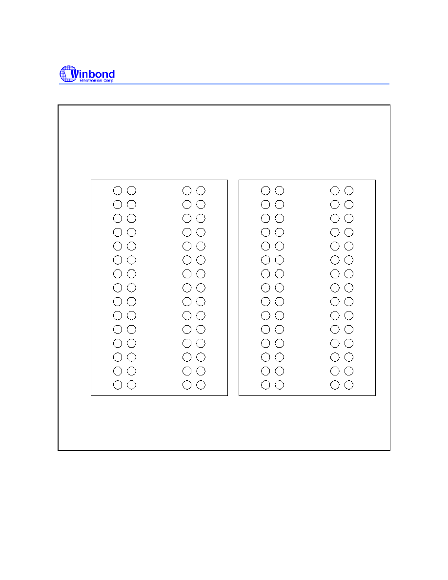
4. PIN CONFIGURATION
Top View
7
6
2
1
C
B
A
P
N
G
D
E
M
H
L
F
K
R
J
VSS
VSS
DQ14
DQ13
DQ12
DQ10
DQ8
NC
NC
NC
CKE
A11
A8
A6
DQ9
DQ15
A4
VSSQ
VDDQ
DQ11
VSSQ
NC
VSS
UDQM
CLK
NC
A9
A7
A5
VDDQ
VDD
VDD
DQ1
DQ2
DQ3
DQ5
DQ7
NC
WE#
CAS#
CS#
BS0
A10
A1
DQ6
DQ0
A3
VDDQ
VSSQ
DQ4
VDDQ
NC
VDD
LDQM
RAS#
NC
BS1
A0
A2
VSSQ
VSS
VSS
DQ14
DQ13
DQ12
DQ10
DQ8
NC
NC
NC
CKE
A11
A8
A6
DQ9
DQ15
A4
VSSQ
VDDQ
DQ11
VSSQ
NC
VSS
UDQM
CLK
NC
A9
A7
A5
VDDQ
VDD
VDD
DQ1
DQ2
DQ3
DQ5
DQ7
NC
WE#
CAS#
CS#
BS0
A10
A1
DQ6
DQ0
A3
VDDQ
VSSQ
DQ4
VDDQ
NC
VDD
LDQM
RAS#
NC
BS1
A0
A2
VSSQ
7 6
2 1
Bottom View
W9864G6DB
Publication Release Date: January 27, 2003
- 5 -
Revision A1
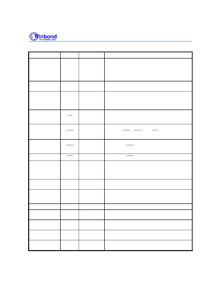
5. PIN DESCRIPTION
BALL LOCATION PIN NAME
FUNCTION
DESCRIPTION
M1, M2, N1, N2,
N6, N7, P1, P2,
P6, P7, R6,
A0
- A11
Address
Multiplexed pins for row and column address. Row
address: A0
- A11. Column address: A0 - A7.
A10 is sampled during a precharge command to
determine if all banks are to be precharged or bank
selected by BS0, BS1.
M6, M7
BS0, BS1 Bank Select
Select bank to activate during row address latch time,
or bank to read/write during address latch time.
A2, A6, B1, B7,
C1, C7, D1, D2,
D6, D7, E1, E7,
F1, F7, G1, G7
DQ0
-
DQ15
Data Input/
Output
Multiplexed pins for data output and input.
L7
CS
Chip Select
Disable or enable the command decoder. When
command decoder is disabled, new command is
ignored and previous operation continues.
K6
RAS
Row Address
Strobe
Command input. When sampled at the rising edge of
the clock
RAS
,
CAS
and
WE
define the
operation to be executed.
K7
CAS
Column
Address
Strobe
Referred to
RAS
J7
WE
Write Enable Referred to
RAS
J6, J5
UDQM
LDQM
Input/Output
Mask
The output buffer is placed at Hi-Z (with latency of 2)
when DQM is sampled high in read cycle. In write
cycle, sampling DQM high will block the write
operation with zero latency.
K2 CLK
Clock
Inputs
System clock used to sample inputs on the rising
edge of clock.
L1 CKE
Clock
Enable
CKE controls the clock activation and deactivation.
When CKE is low, Power Down mode, Suspend
mode, or Self Refresh mode is entered.
A7, H6, R7
V
DD
Power (+3.3V) Power for input buffers and logic circuit inside DRAM.
A1, H2, R1
V
SS
Ground
Ground for input buffers and logic circuit inside
DRAM.
B6, C2, E6, F2
V
DDQ
Power (+3.3V)
for I/O Buffer
Separated power from V
DD
, to improve DQ noise
immunity.
B2, C6, E2, F6
V
SSQ
Ground for I/O
Buffer
Separated ground from V
SS
, to improve DQ noise
immunity.
G2, G6, H1, H7,
J1, K1, L2, L6
NC
No Connection No connection