 | –≠–ª–µ–∫—Ç—Ä–æ–Ω–Ω—ã–π –∫–æ–º–ø–æ–Ω–µ–Ω—Ç: 6N137 | –°–∫–∞—á–∞—Ç—å:  PDF PDF  ZIP ZIP |
19/4/99
DB91063-AAS/A1
6N137
ICPL2601
HIGH CMR, VERY HIGH SPEED
OPTICALLY COUPLED ISOLATOR
LOGIC GATE OUTPUT
ABSOLUTE MAXIMUM RATINGS
(25∞C unless otherwise specified)
Storage Temperature
-55∞C to + 125∞C
Operating Temperature
0∞C to + 70∞C
Lead Soldering Temperature
(1/16 inch (1.6mm) from case for 10 secs) 260∞C
INPUT DIODE
Average Forward Current
20mA
Reverse Voltage
5V
DETECTOR
Enable Input Voltage ( V
E
)
5.5V
(not to exceed V
CC
by more than 500mV)
Reverse Supply Voltage(-V
CC
)
-500mV
Supply Voltage(V
CC
)
7V
(1 minute maximum)
Output Current ( I
O
)
25mA
Output Voltage ( V
O
)
7V
Collector Output Power Dissipation
40mW
APPROVALS
l
UL recognised, File No. E91231
DESCRIPTION
The 6N137 / ICPL2601 optocouplers consist of
a GaAsP light emitting diode and a high gain
integrated photo detector to provide 2500Volts
RMS
electrical isolation between input and output. An
enable input allows the detector to be strobed.
The output of the detector I.C. is an open
collector Schottky clamped transistor. The
ICPL2601 has an internal shield which provides
a guaranteed common mode transient immunity
specification of 1000V/
µ
s minimum.This unique
design provides maximum ac and dc circuit
isolation while achieving TTL compatibility. The
coupled parameters are guaranteed over the
temperature range of 0∞C to 70∞C, such that a
maximum input signal of 5mA will provide a
minimum output sink current of 13mA(equivalent
to fan-out of eight gates)
FEATURES
l
High speed - 10MBit/s
l
High Common Mode Transient
Immunity 10kV/
µ
s typical
l
Logic gate output
l
ICPL2601 has improved noise shield
for superior common mode rejection
l
Options :-
10mm lead spread - add G after part no.
Surface mount - add SM after part no.
Tape&reel - add SMT&R after part no.
APPLICATIONS
l
Line receiver, data transmission
l
Computer-peripheral interface
l
Data multiplexing
l
Pulse transformer replacement
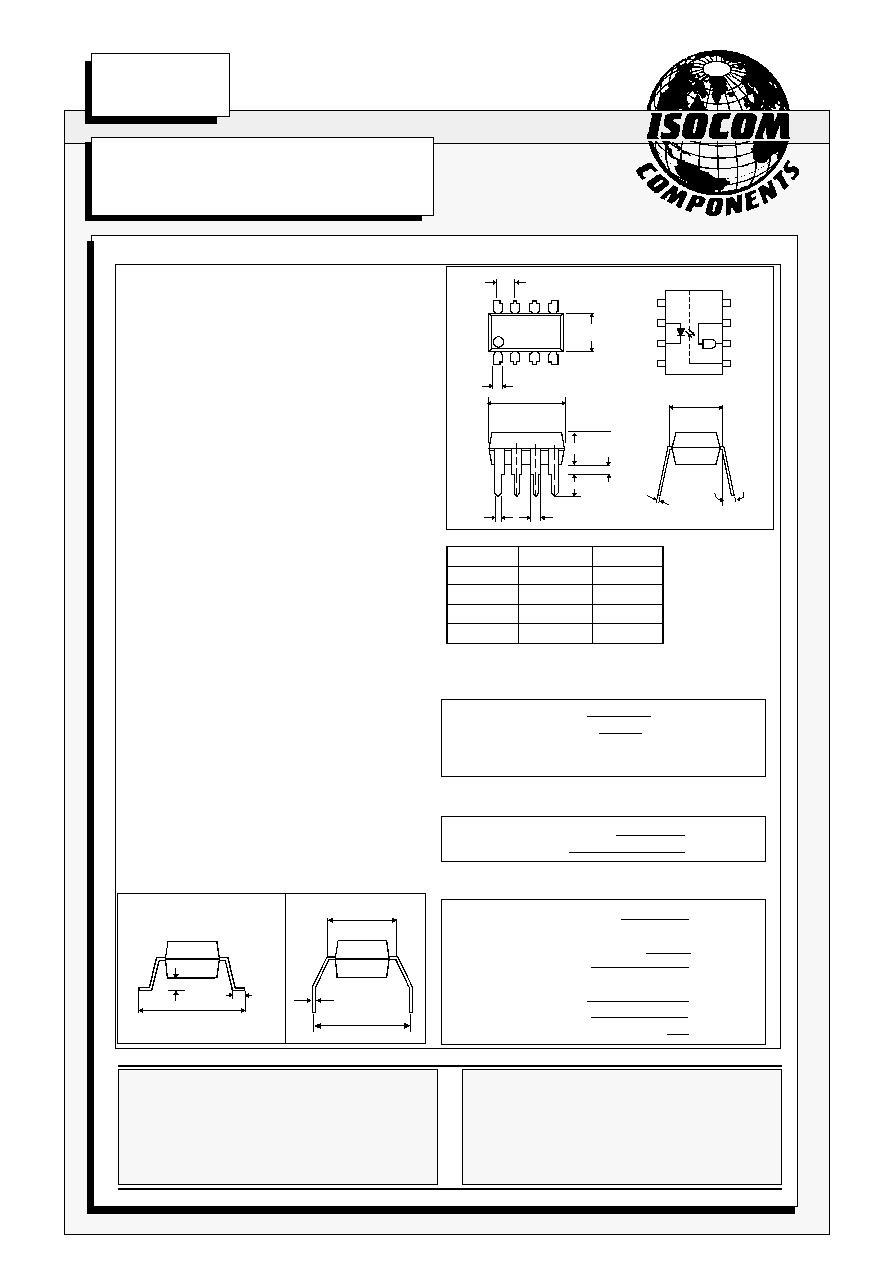
0.3
0.5
Dimensions in mm
6.9
6.3
1.3
15∞
Max
3.3
4.0
3.6
2.54
9.7
9.1
0.5
1.3
* ICPL2601 NOISE SHIELD
7.62
4
3
2
1
8
7
6
5
*
OPTION G
OPTION SM
10.16
10.2
9.5
0.3
1.2
0.6
1.4
0.9
7.62
SURFACE MOUNT
INPUT ENABLE OUTPUT
H
H
L
L
H
H
H
L
H
L
L
H
TRUTH TABLE
A 0.1
µ
F bypass
capacitor must be
connected between
pins 8 and 5 ( See
note 1)
V
CC
GND
ISOCOM INC
1024 S. Greenville Ave, Suite 240,
Allen, TX 75002 USA
Tel: (214) 495-0755 Fax: (214) 495-0901
e-mail info@isocom.com
http://www.isocom.com
ISOCOM COMPONENTS LTD
Unit 25B, Park View Road West,
Park View Industrial Estate, Brenda Road
Hartlepool, TS25 1YD England Tel: (01429)863609
Fax : (01429) 863581 e-mail sales@isocom.co.uk
http://www.isocom.com
DB91063-AAS/A1
19/4/99
ELECTRICAL CHARACTERISTICS ( T
A
= 0∞C to 70∞C Unless otherwise noted )
PARAMETER
SYM DEVICE
MIN TYP* MAX UNITS TEST CONDITION
High Level Output Current
I
OH
0.02
250
µ
A
V
CC
= 5.5V, V
O
= 5.5V
I
F
= 250
µ
A, V
E
= 2V
Low Level Output Voltage
V
OL
0.4
0.6
V
V
CC
= 5.5V, I
F
= 5mA
V
E
= 2V
I
OL
(sinking ) = 13mA
High Level Supply Current
I
CCH
10
15
mA
V
CC
= 5.5V, I
F
= 0mA
V
E
= 0.5V
Low Level Supply Current
I
CCL
15
18
mA
V
CC
= 5.5V, I
F
= 10mA
V
E
= 0.5V
High Level Enable Current
I
EH
-1.0
mA
V
CC
= 5.5V, V
E
= 2V
Low Level Enable Current
I
EL
-1.5
-2.0
mA
V
CC
= 5.5V, V
E
= 0.5V
High Level Enable Voltage
V
EH
2
V
V
CC
= 5.5V, I
F
= 10mA
(note 10)
Low Level Enable Voltage
V
EL
0.8
V
V
CC
= 5.5V, I
F
= 10mA
Input Forward Voltage
V
F
1.55
1.75
V
I
F
= 10mA, T
A
= 25
o
C
Input Reverse Breakdown Voltage
V
BR
5
V
I
R
= 10
µ
A, T
A
= 25
o
C
Input Capacitance
C
IN
60
pF
V
F
= 0, f = 1MHz
Temperature Coefficient
V
F
-1.4
mV/∞C
I
F
= 10mA
of Forward Voltage
T
A
Input-output Isolation Voltage
V
ISO
2500
5000
V
RMS
R.H.equal to or less than
(note 3)
50%, t = 1min, T
A
= 25∞C
Input-output Insulation Leakage
I
I-O
1
µ
A
R.H. = 45%
Current (note 3)
t = 5s, T
A
= 25∞C
V
I-O
= 3000V dc
Resistance (Input to Output)
R
I-O
10
12
V
I-O
= 500V dc
(note 3)
Capacitance (Input to Output)
C
I-O
0.6
pF
f = 1MHz
(note 3)
* All typicals at T
A
= 25∞C
RECOMMMENDED OPERATING CONDITIONS
PARAMETER
SYMBOL
MIN MAX UNITS
Input Current, Low Level
I
FL
0
250
µ
A
Input Current, High Level
I
FH
6.3*
15
mA
Supply Voltage, Output
V
CC
4.5
5.5
V
Enable Voltage, Low Level
V
EL
0
0.8
V
Enable Voltage, High Level
V
EH
2.0
V
CC
V
Fan Out ( TTL Load )
N
8
Operating Temperature
T
A
0
70
∞C
*6.3mA is a guard banded
value which allows for at least
20% CTR degradation.
Initial input current threshold
value is 5.0mA or less
SWITCHING SPECIFICATIONS AT T
A
= 25∞C ( V
CC
= 5V, I
F
= 7.5mA Unless otherwise noted )
PARAMETER
SYM DEVICE
MIN TYP MAX UNITS TEST CONDITION
Propagation Delay Time
to
Logic Low at Output
t
PHL
55
75
ns
R
L
= 350
,
C
L
= 15pF
( fig 1 )( note4 )
Propagation Delay Time
to
Logic High at Output
t
PLH
45
75
ns
R
L
= 350
,
C
L
= 15pF
( fig 1 )( note5 )
Propagation Delay Time
of Enable from V
EH
to V
EL
t
EHL
14
ns
R
L
= 350
,
C
L
= 15pF
( note6 )
V
EL
= 0V, V
EH
= 3V
Propagation Delay Time
of Enable from V
EL
to V
EH
t
ELH
25
ns
R
L
= 350
,
C
L
= 15pF
( note7 )
V
EL
= 0V, V
EH
= 3V
Common Mode Transient
Immunity at Logic High
CM
H
6N137
10000
V/
µ
s
I
F
= 0mA, V
CM
= 50V
PP
Level Output ( fig 2 )( note8 )
ICPL2601 1000 10000
V/
µ
s
R
L
= 350
,
V
OH
= 2Vmin.
Common Mode Transient
Immunity at Logic Low
CM
L
6N137
-10000
V/
µ
s
V
CM
= 50V
PP
Level Output ( fig 2 )( note9 )
ICPL2601 -1000 -10000
V/
µ
s
R
L
=350
,
V
OL
=0.8Vmax.
NOTES:-
1
Bypassing of the power supply line is required, with a 0.01
µ
F ceramic disc capacitor adjacent to
each isolator. The power supply bus for the isolator(s) should be seperate from the bus for any
active loads. Otherwise a larger value of bypass capacitor (up to 0.1
µ
F) may be needed to supress
regenerative feedback via the power supply.
2
Peaking circuits may produce transient input currents up to 50mA, 50ns maximum pulse width,
provided average current does not exceed 20mA.
3
Device considered a two terminal device; pins 1, 2, 3, and 4 shorted together, and pins 5, 6, 7
and 8 shorted together.
4
The t
PHL
propagation delay is measured from the 3.75 mA level Low to High transition of the input
current pulse to the 1.5V level on the High to Low transition of the output voltage pulse.
5
The t
PLH
propagation delay is measured from the 3.75mA level High to Low transition of the input
current pulse to the 1.5V level on the Low to High transition of the output voltage pulse.
6
The t
EHL
enable input propagation delay is measured from the 1.5V level on the Low to High transition of
the enable input voltage pulse to the 1.5V level on the High to Low of the output voltage pulse.
7
The t
ELH
enable input propagation delay is measured from the 1.5V level on the High to Low transition of
the enable input voltage pulse to the 1.5V level on the Low to High of the output voltage pulse.
8
CM
H
is the maximum tolerable rate of rise of the common mode voltage to assure that the output
will remain in a high logic state (ie Vout > 2.0V).
9
CM
L
is the maximum tolerable rate of fall of the common mode voltage to assure that the output
will remain in a low logic state (ie Vout < 0.8V)
10
No external pull up is required for a high logic state on the enable input.
DB91063-AAS/A1
19/4/99
FIG.1 SWITCHING TEST CIRCUIT
2
I
F
Monitor
0
I
F
V
O
1.5V
100
1.5V
5V
t
PHL
t
PLH
V
OL
R
L
V
O
C
L
= 15pF
8
7
6
5
PULSE
GENERATOR
Z
O
= 50
t
r
= 5ns
I
F
1
4
3
10% Duty Cycle
1/f < 100
µ
s
5V

DB91063-AAS/A1
19/4/99
FIG. 2 TEST CIRCUIT FOR TRANSIENT IMMUNITY AND TYPICAL WAVEFORMS
1
3
4
+
-
A
PULSE GEN.
V
CM
0V
V
CM
I
F
V
FF
5V
5V
V
OL
V
O
V
O
SWITCH AT A: I
F
= 0mA
SWITCH AT B: I
F
= 7.5mA
10V
10%
90%
10%
90%
t
r
t
f
B
8
7
6
5
2
R
L
V
O
Output voltage V
O
(V)
Output Voltage vs.
Forward Input Current
1.0 1.2 1.4 1.6
Forward current I
F
(mA)
Forward Current vs. Forward
Voltage
Forward voltage V
F
(V)
Low Level Output Voltage vs.
Ambient Temperature
Low level output voltage V
OL
(V)
Ambient temperature T
A
( ∞C )
0 10 20 30 40 50 60 70
High level output current I
OH
(
µ
A )
0 1 2 3 4 5 6
Forward input current I
F
(mA)
High Level Output Current vs.
Ambient Temperature
0.01
0.1
0.02
0.04
0.2
0.4
1
2
4
10
T
A
= 25∞C
0
0.001
0.002
0.004
0.01
0.02
0.04
0.1
0.2
0.4
1.0
V
CC
= 5V
T
A
= 25∞C
0
1
2
3
4
5
6
7
8
9
V
CC
R
L
= 1k
R
L
= 350
V
CC
= 5.5V
V
E
= 2V
I
F
= 5mA
I
O
= 12.8mA
I
O
= 16mA
I
O
= 6.4mA
I
O
= 9.6mA
0.1
0.2
0.3
0.4
0.5
0.6
0.7
0.8
V
CC
= 5.5V
V
O
= 5.5V
V
E
= 2V
I
F
= 250
µ
A
0 10 20 30 40 50 60 70
Ambient temperature T
A
( ∞C )