ISOCOM COMPONENTS LTD
Unit 25B, Park View Road West,
Park View Industrial Estate, Brenda Road
Hartlepool, Cleveland, TS25 1YD
Tel: (01429) 863609 Fax :(01429) 863581
13/12/00
DB92513-AAS/A1
7.62
APPROVALS
l
UL recognised, File No. E91231
'X' SPECIFICATION APPROVALS
l
l
VDE 0884 approval pending
l
EN60950 approval pending
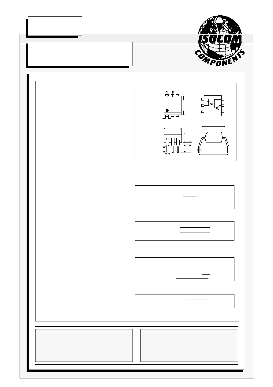
DESCRIPTION
The CNX83AG optically coupled isolator
consists of an infrared light emitting diode and
a NPN silicon photo transistor in a standard 6
pin dual in line plastic package.
FEATURES
l
High Current Transfer Ratio (40% min)
l
Low Saturation Voltage suitable for TTL
integrated circuits
l
High BV
CEO
(50V min)
l
High Isolation Voltage (5.3kV
RMS
,7.5kV
PK
)
APPLICATIONS
l
DC motor controllers
l
Industrial systems controllers
l
Signal transmission between systems of
different potentials and impedances
0.5
Dimensions in mm
10.16
7.0
6.0
1.2
3.0
3.35
4.0
3.0
2.54
0.26
7.62
6.62
0.5
1
3
4
6
2
5
ABSOLUTE MAXIMUM RATINGS
(25∞C unless otherwise specified)
Storage Temperature
-55∞C to + 150∞C
Operating Temperature
-55∞C to + 100∞C
Lead Soldering Temperature
(1/16 inch (1.6mm) from case for 10 secs) 260∞C
INPUT DIODE
Forward Current
60mA
Reverse Voltage
6V
Power Dissipation
105mW
OUTPUT TRANSISTOR
Collector-emitter Voltage BV
CEO
50V
Collector-base Voltage BV
CBO
70V
Emitter-collector Voltage BV
ECO
6V
Power Dissipation
160mW
POWER DISSIPATION
Total Power Dissipation
200mW
(derate linearly 2.67mW/∞C above 25∞C)
OPTICALLY COUPLED
ISOLATOR
PHOTOTRANSISTOR OUTPUT
CNX83AG
ISOCOM INC
1024 S. Greenville Ave, Suite 240,
Allen, TX 75002 USA
Tel: (214) 495-0755 Fax: (214) 495-0901
e-mail info@isocom.com
http://www.isocom.com

DB92513-AAS/A1
13/12/00
PARAMETER
MIN TYP MAX UNITS TEST CONDITION
Input
Forward Voltage (V
F
)
1.2
1.5
V
I
F
= 10mA
Reverse Voltage (V
R
)
6
V
I
R
= 10
µ
A
Reverse Current (I
R
)
10
µ
A
V
R
= 6V
Output
Collector-emitter Breakdown (BV
CEO
)
50
V
I
C
= 1mA
( Note 2 )
Collector-base Breakdown (BV
CBO
)
70
V
I
C
= 100
µ
A
Emitter-collector Breakdown (BV
ECO
)
6
V
I
E
= 100
µ
A
Collector-emitter Dark Current (I
CEO
)
50
nA
V
CE
= 10V
Coupled
Current Transfer Ratio (I
C
/ I
F
)
(Note 2)
0.4
10mA I
F
, 0.4V V
CE
1.5
10mA I
F
, 5V V
CE
Collector-emitter Saturation VoltageV
CE
(SAT)
0.4
V
10mA I
F
, 4mA I
C
Input to Output Isolation Voltage V
ISO
5300
V
RMS
See note 1
7500
V
PK
See note 1
Input-output Isolation Resistance R
ISO
5x10
10
V
IO
= 500V (note 1)
Turn-on Time
t
on
3
µ
s
V
CC
= 5V , I
C
= 2mA ,
Turn-off Time
t
off
3
µ
s
R
L
= 100
Turn-on Time
t
on
12
µ
s
V
CC
= 5V , I
C
= 2mA ,
Turn-off Time
t
off
12
µ
s
R
L
= 1k
Note 1
Measured with input leads shorted together and output leads shorted together.
Note 2
Special Selections are available on request. Please consult the factory.
ELECTRICAL CHARACTERISTICS ( T
A
= 25∞C Unless otherwise noted )

DB92513-AAS/A1
13/12/00
50
Ambient temperature T
A
( ∞C )
150
0
200
Ambient temperature T
A
( ∞C )
Collector power dissipation P
C
(mW)
60
30
20
10
0
40
50
-30 0 25 50 75 100 125
Collector Power Dissipation vs. Ambient Temperature
Forward Current vs. Ambient Temperature
-30 0 25 50 75 100
100
0
0.5
1.0
1.5
I
F
= 10mA
V
CE
= 0.4V
Forward current I
F
(mA)
Relative Current Transfer Ratio
vs. Ambient Temperature
Relative current transfer ratio
70
80
1 2 5 10 20 50
0
0.8
1.2
1.6
2.0
2.4
0.4
2.8
V
CE
= 0.4V
T
A
= 25∞C
Relative current transfer ratio
Relative Current Transfer Ratio
vs. Forward Current
Forward current I
F
(mA)
Collector Current vs. Collector-emitter Voltage
Collector-emitter voltage V
CE
( V )
Collector current I
C
(mA)
0 2 4 6 8 10
0
10
20
30
40
50
T
A
= 25∞C
I
F
= 5mA
10
15
20
30
50
-30 0 25 50 75 100 125
Ambient temperature T
A
( ∞C )
Collector-emitter saturation voltage V
CE(S
A
T)
(V)
Collector-emitter Saturation
Voltage vs. Ambient Temperature
0
0.04
0.08
0.12
0.16
0.20
0.24
0.28
I
F
= 10mA
I
C
= 4mA
-30 0 25 50 75 100
Ambient temperature T
A
( ∞C )