ISOCOM COMPONENTS LTD
Unit 25B, Park View Road West,
Park View Industrial Estate, Brenda Road
Hartlepool, Cleveland, TS25 1YD
Tel: (01429) 863609 Fax :(01429) 863581
HIGH DENSITY MOUNTING
PHOTODARLINGTON
OPTICALLY COUPLED ISOLATORS
DESCRIPTION
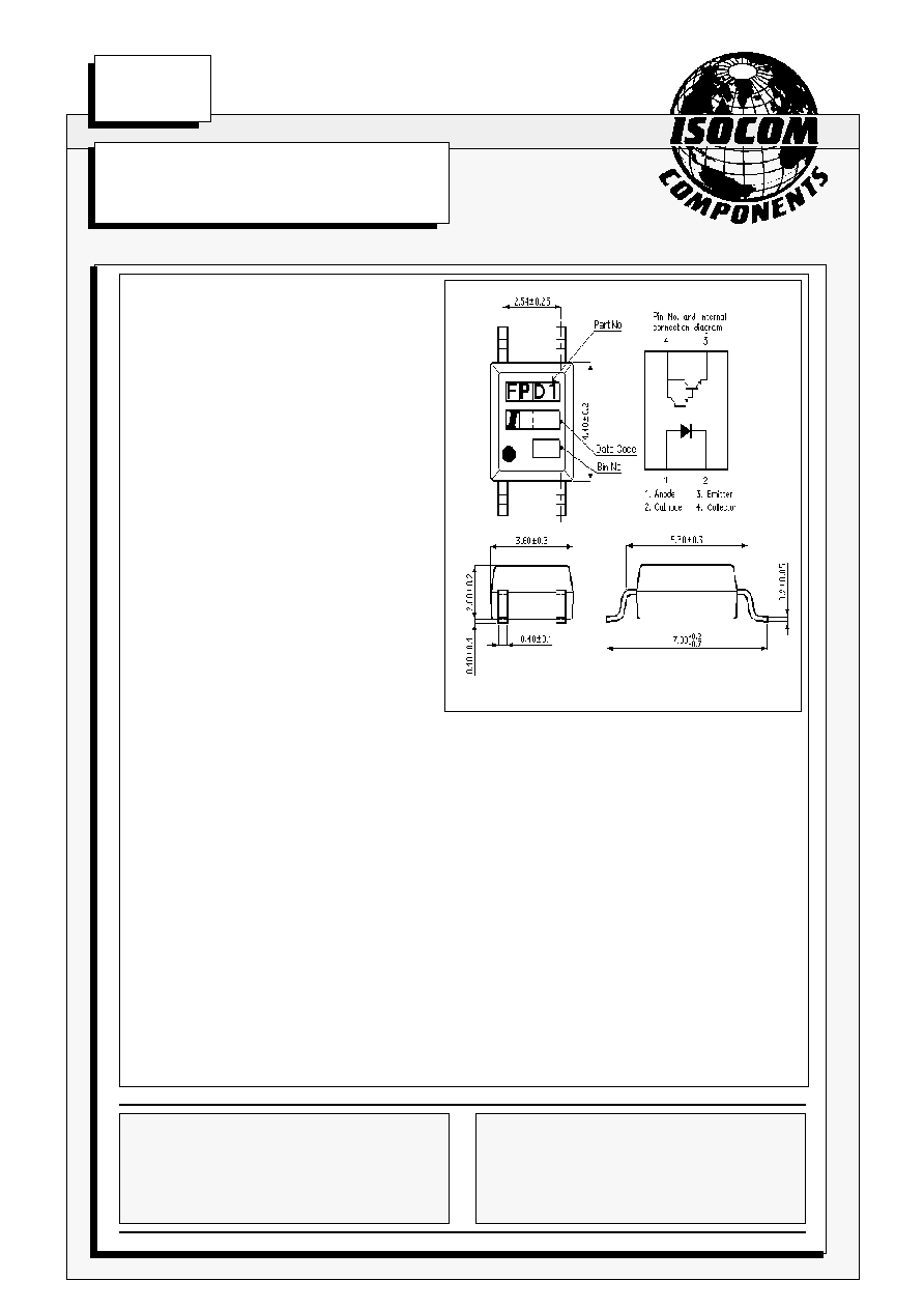
The IS355 is an optically coupled isolator
consisting of an infrared light emitting diode and
NPN silicon photodarlington in a space efficient
dual in line plastic package.
FEATURES
l
Marked as FPD1.
l
Current Transfer Ratio MIN. 600%
l
Isolation Voltage (3.75kV
RMS
,5.3kV
PK
)
l
All electrical parameters 100% tested
l
Drop in replacement for Sharp PC355
APPLICATIONS
l
Computer terminals
l
Industrial systems controllers
l
Measuring instruments
l
Signal transmission between systems of
different potentials and impedances
ISOCOM INC
1024 S. Greenville Ave, Suite 240,
Allen, TX 75002 USA
Tel: (214) 495-0755 Fax: (214) 495-0901
e-mail info@isocom.com
http://www.isocom.com
IS355
DB92859l-AAS/A3
22/4/02
Dimensions in mm
PARAMETER
MIN TYP MAX UNITS TEST CONDITION
Input
Forward Voltage (V
F
)
1.2
1.4
V
I
F
= 20mA
Reverse Voltage (V
R
)
5
V
I
R
= 10
�
A
Reverse Current (I
R
)
10
�
A
V
R
= 4V
Output
Collector-emitter Breakdown (BV
CEO
)
35
V
I
C
= 0.1mA
Emitter-collector Breakdown (BV
ECO
)
6
V
I
E
= 10uA
Collector-emitter Dark Current (I
CEO
)
1
uA
V
CE
= 10V
Coupled
Current Transfer Ratio (CTR)
600
7500
%
1mA I
F
, 2V V
CE
Collector-emitter Saturation VoltageV
CE
(SAT)
1
V
20mA I
F
, 1mA I
C
Input to Output Isolation Voltage V
ISO
3750
V
RMS
See note 1
5300
V
PK
See note 1
Input-output Isolation Resistance R
ISO
5x10
10
V
IO
= 500V (note 1)
Output Rise Time
tr
4
18
�
s
V
CE
= 2V ,
Output Fall Time
tf
3
18
�
s
I
C
= 2mA, R
L
= 100
ELECTRICAL CHARACTERISTICS ( T
A
= 25�C Unless otherwise noted )
ABSOLUTE MAXIMUM RATINGS
(25�C unless otherwise specified)
Storage Temperature
-55�C to + 150�C
Operating Temperature
-55�C to + 100�C
Lead Soldering Temperature
(1/16 inch (1.6mm) from case for 10 secs) 260�C
INPUT DIODE
Forward Current
50mA
Reverse Voltage
6V
Power Dissipation
70mW
OUTPUT TRANSISTOR
Collector-emitter Voltage BV
CEO
35V
Emitter-collector Voltage BV
ECO
6V
Power Dissipation
150mW
POWER DISSIPATION
Total Power Dissipation
170mW
(derate linearly 2.26mW/�C above 25�C)
Note 1
Measured with input leads shorted together and output leads shorted together.
DB92859l-AAS/A3
22/4/02
12/07/01 Appendix to Mini Flat Pack FPD-AAS/A1
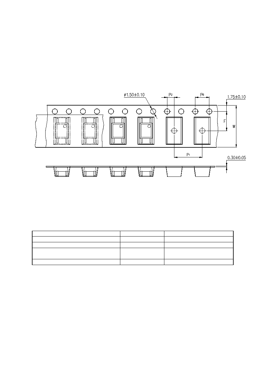
TAPING DIMENSIONS
Description
Symbol
Dimensions in mm ( inches )
Tape wide
W
12
�
0.3 ( .47 )
Pitch of sprocket holes
P
0
4
�
0.1 ( .15 )
Distance of compartment
F
P
2
5.5
�
0.1 ( .217 )
2
�
0.1 ( .079 )
Distance of compartment to compartment
P
1
8
�
0.1 ( .315 )

12/07/01 Appendix to Mini Flat Pack FPD-AAS/A1
CHARACTERISTIC CURVES
Fig.1 Forward Current vs. Ambient
Fig.2 Collector Power Dissipation vs.
Ambient Temperature
Fig.4 Forward Current vs. Forward
Fig.5 Current Transfer Ratio vs. Forward
Current
Fig.6 Collector Current vs.
Collector-emitter Voltage
0
0
Ta= 75 C
50 C
25 C
0 C
-25 C
Ta= 25 C
Pc(MAX.)
5mA
2mA
1mA
Fig.3 Collector-emitter Saturation
Voltage vs. Forward Current
Ic
=
0.5
mA
1mA
3mA
7mA
5mA
Ta= 25 C
30mA
Temperature
o
o
10
20
30
40
50
60
0
50
100
150
200
0
0
0.5 1.0 1.5 2.0 2.5
4.0
3.0 3.5
1
2
3
4
5
6
7
8
o
0
1
0.5
1.0
3.0
1.5
2.0
2.5
2
5
10
20
50
100
200
500
o
o
o
o
o
0
0.1
0.2
0.5
1
2
5
10
1000
2000
3000
4000
5000
0
20
40
60
80
100
1
2
3
4
5
O
O
Voltage
I
F
= 10mA
Forward current I
F
(mA)
Collector-emitter voltage V
CE
(V)
Forward voltage V
F
(V)
Ambient temperature Ta ( C)
Forward current I
F
(mA)
Ambient temperature Ta ( C)
Forward current I
F
(mA)
Collector power dissipation Pc (mW)
Forward current I
F
(mA)
Currentor-emitter saturation voltage
V
CE
(sat)
Collector current I
C
(mA)
Current transfer ratio CTR (
%)
V
CE
= 2V
Ta= 25 C
0
50
25
75
100
125
-55
-55
125
25
0
50
75
100

12/07/01 Appendix to Mini Flat Pack FPD-AAS/A1
CHARACTERISTIC CURVES
Fig.7 Relative Current Transfer Ratio
vs. Ambient Temperature
Fig.8 Collector-emitter Saturation Voltage
Fig.9 Collector Dark Current vs.
Ambient Temperature
Fig.10 Response Time vs. Load
Fig.11 Frequency Response
0
Ta= 25 C
tr
tf
td
ts
vs. Ambient Temperature
Ambient temperature Ta ( C)
Ambient temperature Ta ( C)
Ambient temperature Ta ( C)
Frequency f (kHz)
o
o
o
o
o
40
60
80
100
50
100
150
0
0.2
0.4
0.6
0.8
1.0
20
40
60
80
100
0.2
0.05
40
60
80
100
0.1 0.2
0.5
1
2
5
10
0.5
1
2
5
10
20
50
100
200
500
0.02
-20
-10
0
0.1
10
100
1
Resistance
Test Circuit for Response Time
Test Circuit for Frequency Response
Input
Output
Input
Output
Vcc
td
tr
tf
ts
90%
10%
Collecotr dark current I
CEO
(nA)
Relative current transfer ratio (
%)
Response time (
s)
Voltage gain Av (dB)
Load resistance R
L
(k
)
R
L
R
D
R
L
R
D
Output
Vcc
I
F
= 1mA
V
CE
= 2V
I
F
= 20mA
I
C
= 1mA
V
CE
= 2V
I
C
= 10mA
V
CE
= 2V
I
C
= 2mA
Ta= 25 C
20
1
10
100
1000
10000
100000
20
R
L
= 10k
1k
100
Collector-emitter saturation voltage
V
CE
(sat) (V)
V
CE
= 20V
12/07/01 Appendix to Mini Flat Pack FPD-AAS/A1
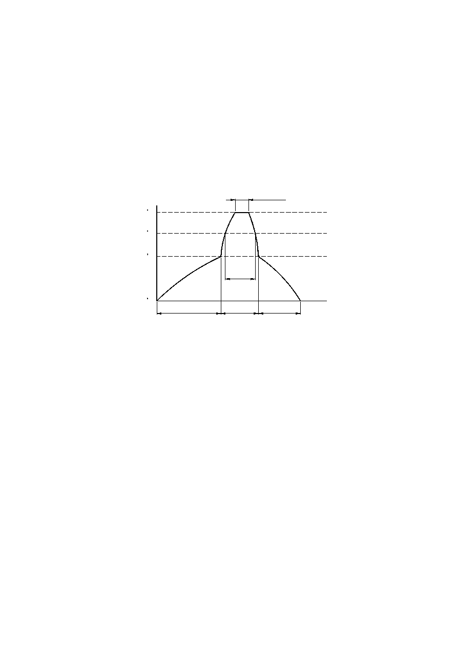
TEMPERATURE PROFILE OF SOLDERING REFLOW
(1) One time soldering reflow is recommended within the condition of temperature and time profile
shown below.
30 seconds
1 minute
2 minutes
1.5 minutes
1 minute
25 C
180 C
200 C
230 C
(2) When using another soldering method such as infrated ray lamp, the temperature may rise
partially in the mold of the device.
Keep the temperature on the package of the device within the condition of above (1).