ISOCOM COMPONENTS LTD
Unit 25B, Park View Road West,
Park View Industrial Estate, Brenda Road
Hartlepool, Cleveland, TS25 1YD
Tel: (01429) 863609 Fax :(01429) 863581
11/12/00
DB91024m-AAS/A2
APPROVALS
l
UL recognised, File No. E91231
DESCRIPTION
The IS4N45, IS4N46 are optically coupled
isolators consisting of an infrared light emitting
diode and a NPN silicon photo darlington which
has an integral base-emitter resistor to optimise
switching speed and elevated temperature
characteristics in a standard 6pin dual in line
plastic package. These devices are designed to
equal the 4N45, 4N46 characteristics while
providing greater voltage and current capability.
FEATURES
l
Options :-
10mm lead spread - add G after part no.
Surface mount - add SM after part no.
Tape&reel - add SMT&R after part no.
l
High Isolation Voltage (5.3kV
RMS
,7.5kV
PK
)
l
High Current Transfer Ratio ( 1500% typ.)
l
High BV
CEO
( 55V min.)
l
Internal base-emitter resistor minimizes
output leakage
l
Low input current 0.5mA I
F
APPLICATIONS
l
Telephone ring detector
l
Digital logic ground isolation
l
Low input current line receiver
l
Logic to reed relay interface
l
Level shifting
l
Interface between logic families
l
Line voltage status indicator - low input
power dissipation
IS4N46
IS4N45
LOW INPUT CURRENT
DARLINGTON OUTPUT OPTICALLY
COUPLED ISOLATOR
ABSOLUTE MAXIMUM RATINGS
(25∞C unless otherwise specified)
Storage Temperature
-55∞C to + 150∞C
Operating Temperature
-55∞C to + 100∞C
Lead Soldering Temperature
(1/16 inch (1.6mm) from case for 10 secs) 260∞C
INPUT DIODE
Forward Current
60mA
Reverse Voltage
6V
Peak Forward Current
3A
(1
µ
s pulse, 300pps)
Power Dissipation
100mW
OUTPUT TRANSISTOR
Output Voltage ( pin 5 - 4 ) V
O
55V
Emitter-baseVoltage (pin 4 - 6)
7V
Power Dissipation
200mW
POWER DISSIPATION
Total Power Dissipation
260mW
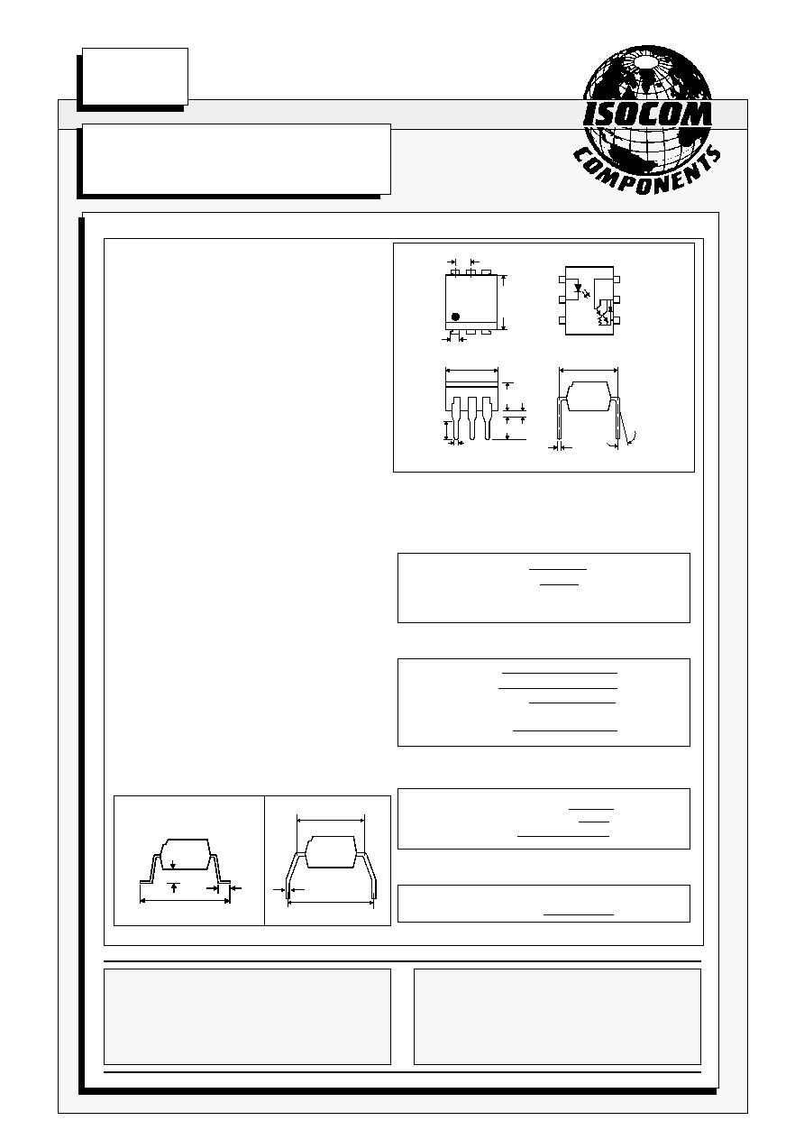
Dimensions in mm
1
3
4
6
2
5
0.5
0.26
0.5
7.0
6.0
1.2
7.62
3.0
13∞
Max
3.35
4.0
3.0
2.54
7.62
6.62
ISOCOM INC
1024 S. Greenville Ave, Suite 240,
Allen, TX 75002 USA
Tel: (214) 495-0755 Fax: (214) 495-0901
e-mail info@isocom.com
http://www.isocom.com
OPTION G
7.62
SURFACE MOUNT
OPTION SM
10.16
0.26
10.46
9.86
0.6
0.1
1.25
0.75
DB91024m-AAS/A1
11/12/00
PARAMETER
MIN TYP MAX UNITS TEST CONDITION
Input
Forward Voltage (V
F
)
1.2
1.5
V
I
F
= 10mA
Reverse Voltage (V
R
)
6
V
I
R
= 10
µ
A
Reverse Current (I
R
)
10
µ
A
V
R
= 6V
Output
Output Breakdown Voltage ( pin 5 - 4)
55
V
I
54
= 1mA
Base Breakdown ( pin 4 - 6 )
7
V
I
E
= 0.1mA
Logic High Output
100
µ
A
V
54
= 18V
Coupled
DC Current Transfer Ratio ( CTR )
IS4N46
350
%
0.5mA I
F
, 1V V
CE
IS4N46
500
%
1mA I
F
, 1V V
CE
IS4N45
250
%
1mA I
F
, 1V V
CE
IS4N46, IS4N45
200
%
10mA I
F
, 1.2V V
CE
Logic Low Output Voltage ( V
OL
)
IS4N46
1.0
V
0.5mA I
F
, 1.75mA I
OL
IS4N46
1.0
V
1mA I
F
, 5mA I
OL
IS4N45
1.0
V
1mA I
F
, 2.5mA I
OL
IS4N46, IS4N45
1.2
V
10mA I
F
, 20mA I
OL
Input to Output Isolation Voltage V
ISO
5300
V
RMS
See note 1
7500
V
PK
See note 1
Input-output Isolation Resistance R
ISO
10
11
V
IO
= 500V (note 1)
Input-output Capacitance
Cf
0.5
pF
V = 0, f =1MHz
ELECTRICAL CHARACTERISTICS ( T
A
= 25∞C Unless otherwise noted )
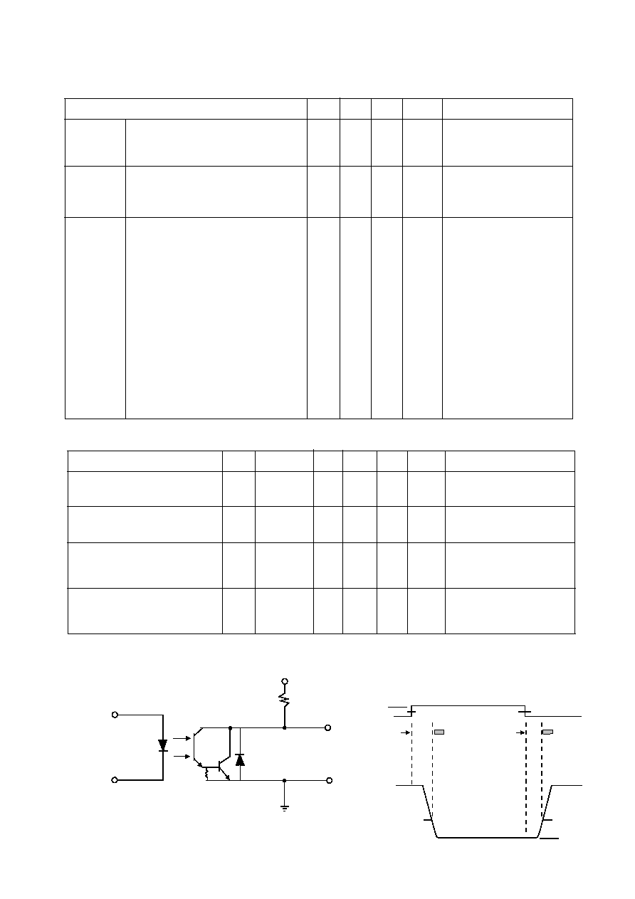
Output
V
CC
Input
FIGURE 1
R
L
SWITCHING SPECIFICATIONS AT T
A
= 25∞C ( V
CC
= 5V Unless otherwise noted )
PARAMETER
SYM DEVICE
MIN TYP MAX UNITS
TEST CONDITION
Propagation Delay Time
t
PHL
IS4N46,45
80
µ
s
I
F
= 1mA, R
L
= 10k
to
Logic Low at Output ( fig.1)
t
PHL
IS4N46,45
5
50
µ
s
I
F
= 10mA, R
L
= 220
Propagation Delay Time
t
PLH
IS4N46,45
1500
µ
s
I
F
= 1mA, R
L
= 10k
to
Logic High at Output( fig.1)
t
PLH
IS4N46,45
150
500
µ
s
I
F
= 10mA, R
L
= 220
Common Mode Transient
Immunity at Logic High
CM
H
500
V/
µ
s
I
F
= 0mA,V
CM
= 10V
PP
Level Output
R
L
= 10k
Common Mode Transient
Immunity at Logic Low
CM
L
500
V/
µ
s
I
F
= 1mA,V
CM
= 10V
PP
Level Output
R
L
= 10k
t
PHL
t
PLH
I
F
0
V
O
V
O
2.5V
2.5V
V
OL
5V
DB91024m-AAS/A1
11/12/00
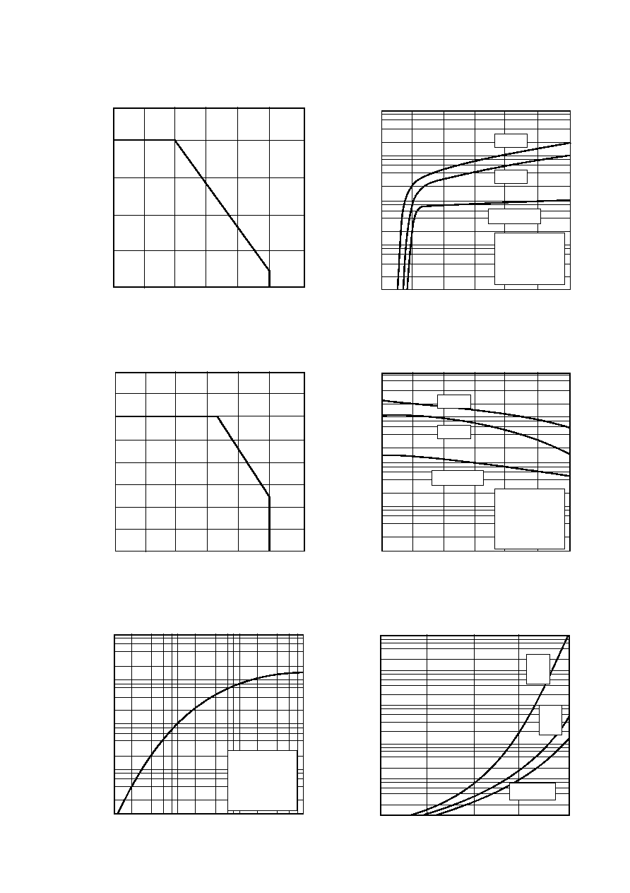
0 1 2 3 4 5 6
0.01
0.1
Collector-emitter voltage V
CE
( V )
-30 0 25 50 75 100
Ambient temperature T
A
( ∞C )
Normalized Output Current vs.
Collector-emitter Voltage
Collector dark current I
CEO
(nA)
Collector Dark Current vs.
Ambient Temperature
-30 0 25 50 75 100 125
Ambient temperature T
A
( ∞C )
100
0
Collector power dissipation P
C
(mW)
Collector Power Dissipation vs. Ambient Temperature
50
0.1 1.0 10 100
Input current I
F
(mA)
Normalized Output Current vs.
Input Current
0.01
0.1
1.0
10
1.0
10
100
Normalized output current
I
F
= 1mA
10mA
50mA
1
10
100
1k
10k
100k
150
200
250
1.0
Normalized output current
Normalized Output Current vs.
Ambient Temperature
10
-50 -25 0 25 50 75 100
Ambient temperature T
A
( ∞C )
Ambient temperature T
A
( ∞C )
60
30
20
10
0
40
50
-30 0 25 50 75 100 125
Forward Current vs. Ambient Temperature
Forward current I
F
(mA)
70
80
Normalized to
I
F
= 1mA
(300
µ
s pulse),
V
CE
= 5V
10mA
I
F
= 1mA
50mA
Normalized to
I
F
= 1mA
(300
µ
s pulse),
V
CE
= 5V
T
A
= 25 ∞C
0.01
Normalized output current
50V
V
CE
V
CE
= 5V
0.1
100
100
Normalized to
I
F
= 1mA
(300
µ
s pulse),
V
CE
= 5V
T
A
= 25 ∞C
10V
V
CE