ISOCOM COMPONENTS LTD
Unit 25B, Park View Road West,
Park View Industrial Estate, Brenda Road
Hartlepool, Cleveland, TS25 1YD
Tel: (01429) 863609 Fax :(01429) 863581
7/12/00
DB92102-AAS/A2
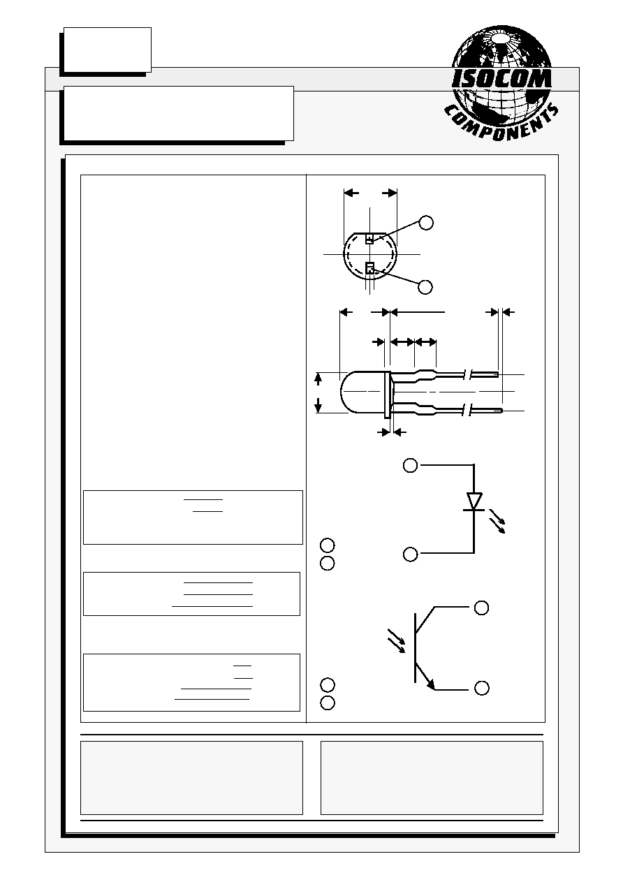
3mm DIA. MATCHED INFRARED
EMITTER DETECTOR PAIR
PHOTOTRANSISTOR OUTPUT
IS654A
IS655A
Dimensions in mm
ABSOLUTE MAXIMUM RATINGS
(25∞C unless otherwise specified)
Storage Temperature
-40∞C to + 85∞C
Operating Temperature
-25∞C to + 85∞C
Lead Soldering Temperature
(1/16 inch (1.6mm) from case for 10 secs) 260∞C
INPUT DIODE
Forward Current
60mA
Reverse Voltage
5V
Power Dissipation
90mW
OUTPUT TRANSISTOR
Collector-emitter Voltage BV
CEO
30V
Emitter-collector Voltage BV
ECO
5V
Collector Current I
C
20mA
Power Dissipation
50mW
DESCRIPTION
The IS654A ( Gallium Arsenide Emitting
Diode ) and the IS655A ( NPN Silicon Photo
Transistor ) are a mechanically and spectrally
matched emitter detector end looking pair.
FEATURES
l
T-1 standard 3mm DIA.
l
Detector has dark plastic package for
visible light cut out
l
LED has high output, Radiant Intensity :-
I
E
= 2mW/sr min. at I
F
= 20mA
l
All electrical parameters are 100% tested
APPLICATIONS
l
Floppy disk drives
l
Infrared applied systems
l
VCRs, Video camera
l
Optoelectronic switches
2
4.0
1
5.3
1.0 min.
12.7min.
1.0
1.5
max
2.6
1.5
3.0
1
2
1
2
IS654A
1
2
- Anode
- Cathode
IS655A
1
2
- Emitter
- Collector
ISOCOM INC
1024 S. Greenville Ave, Suite 240,
Allen, TX 75002 USA
Tel: (214) 495-0755 Fax: (214) 495-0901
e-mail info@isocom.com
http://www.isocom.com
DB92102-AAS/A2
7/12/00
PARAMETER
MIN TYP MAX UNITS TEST CONDITION
IS654A
Forward Voltage (V
F
)
1.2
1.6
V
I
F
= 20mA
Emitter
Reverse Current (I
R
)
100
µ
A
V
R
= 5V
Radiant Flux (I
E
)
1.5
mW/sr
I
F
= 40mA
Peak Emission Wavelength
940
nm
I
F
= 40mA
Spectrum Radiation Bandwidth
50
nm
I
F
= 40mA
Beam Emission Angle
±20
deg.
IS655A
Collector-emitter Breakdown (BV
CEO
)
30
V
I
C
= 1mA
Detector
( Note 1 )
Ee = 0mW/cm
2
Emitter-collector Breakdown (BV
ECO
)
5
V
I
E
= 100
µ
A
Ee = 0mW/cm
2
Collector-emitter Dark Current (I
CEO
)
100
nA
V
CE
= 10V
Ee = 0mW/cm
2
On-State Collector Current I
C
(
ON
)
1
mA
5V V
CE
Ee = 1mW/cm
2
Collector-emitter Saturation Voltage V
CE(SAT)
0.4
V
I
C
= 0.5mA
Ee = 0.5mW/cm
2
Rise Time
tr
10
40
µ
s
V
CC
= 20V, I
C
= 1mA,
Fall Time
tf
8
35
µ
s
R
L
= 1k
Peak Sensitivity Wavelength
940
nm
I
F
= 40mA
Beam Acceptance Angle
±20
deg.
ELECTRICAL CHARACTERISTICS ( T
A
= 25∞C Unless otherwise noted )
Note 1
Special Selections are available on request. Please consult the factory.

DB92102-AAS/A2
7/12/00
0
0.5
1.5
Forward current I
F
(mA)
0 20 40 60 80 100
0 1 2 3 4 5
Irradiance Ee ( mW/cm
2
)
Relative collector current
Relative Collector Current vs.
Irradiance
0
1.0
2.0
3.0
4.0
5.0
V
CE
= 5V
Relative Radiant Intensity vs.
Forward Current
Relative radiant intensity
Ambient temperature T
A
( ∞C )
Forward Current vs. Ambient
Temperature
Forward current I
F
(mA)
60
30
20
10
0
40
50
-25 0 25 50 75 100 125
70
80
10
-25 0 25 50 75 100 125
Ambient temperature T
A
( ∞C )
30
0
40
Collector power dissipation P
C
(mW)
Collector Power Dissipation vs.
Ambient Temperature
20
50
60
0
0.5
Wavelength (nm)
840 940 1040
0 1 2 3 4 5 6 7 8 9 10
Load resistance R
L
(k
)
Rise and fall time tr, tf (
µ
s)
Rise and Fall Time vs.
Load Resistance
0
10
20
30
40
50
60
70
V
CC
= 20V
I
C
= 1mA
T
A
= 25∞C
Spectral Distribution
Relative radiant intensity
2.0
tf
tr
80
90
100
1.0
1.0
2.5