ISOCOM COMPONENTS LTD
Unit 25B, Park View Road West,
Park View Industrial Estate, Brenda Road
Hartlepool, Cleveland, TS25 1YD
Tel: (01429) 863609 Fax :(01429) 863581
7/12/00
DB92260m-AAS/A1
APPROVALS
l
UL recognised, File No. E91231
DESCRIPTION
The IS66_ series are optically coupled isolators
consisting of infrared light emitting diode and a
high voltage NPN silicon photo darlington which
has an integral base-emitter resistor to optimise
switching speed and elevated temperature
characteristics in a standard 6pin dual in line
plastic package.
FEATURES
l
Options :-
10mm lead spread - add G after part no.
Surface mount - add SM after part no.
Tape&reel - add SMT&R after part no.
l
High Isolation Voltage (5.3kV
RMS
,7.5kV
PK
)
l
High Current Transfer Ratio ( 1000% min)
l
High BV
CEO
(400V min. - IS662)
(300V min. - IS661)
(200V min. - IS660)
l
Low collector dark current :-
1
�
A max. at 200V V
CE
- IS661, IS662
1
�
A max. at 100V V
CE
- IS660
l
Low input current 1mA I
F
APPLICATIONS
l
Modems
l
Copiers, facsimiles
l
Numerical control machines
l
Signal transmission between systems of
different potentials and impedances
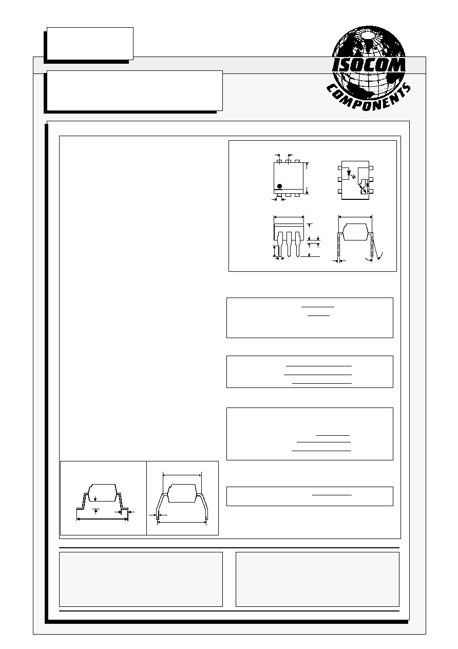
IS660, IS661, IS662
HIGH VOLTAGE DARLINGTON
OUTPUT OPTICALLY COUPLED
ISOLATOR
ABSOLUTE MAXIMUM RATINGS
(25�C unless otherwise specified)
Storage Temperature
-55�C to + 150�C
Operating Temperature
-55�C to + 100�C
Lead Soldering Temperature
(1/16 inch (1.6mm) from case for 10 secs) 260�C
INPUT DIODE
Forward Current
50mA
Reverse Voltage
6V
Power Dissipation
70mW
OUTPUT TRANSISTOR
Collector-emitter Voltage BV
CEO
200, 300, 400V
Collector-base Voltage BV
CBO
200, 300, 400V
Emitter-baseVoltage BV
ECO
6V
Collector Current I
C
150mA
Power Dissipation
300mW
POWER DISSIPATION
Total Power Dissipation
350mW
10.16
0.26
OPTION G
7.62
OPTION SM
SURFACE MOUNT
0.26
0.5
Dimensions in mm
7.0
6.0
1.2
7.62
3.0
13�
Max
3.35
4.0
3.0
2.54
7.62
6.62
0.5
1
3
4
6
2
5
10.46
9.86
0.6
0.1
1.25
0.75
ISOCOM INC
1024 S. Greenville Ave, Suite 240,
Allen, TX 75002 USA
Tel: (214) 495-0755 Fax: (214) 495-0901
e-mail info@isocom.com
http://www.isocom.com

DB92260m-AAS/A1
PARAMETER
MIN TYP MAX UNITS TEST CONDITION
Input
Forward Voltage (V
F
)
1.2
1.4
V
I
F
= 10mA
Reverse Voltage (V
R
)
6
V
I
R
= 10
�
A
Reverse Current (I
R
)
10
�
A
V
R
= 6V
Output
Collector-emitter Breakdown (BV
CEO
)
IS660
200
V
I
C
= 1mA
IS661
300
V
I
C
= 1mA
IS662
400
V
I
C
= 1mA
Collector-base Breakdown (BV
CBO
)
IS660
200
V
I
C
= 0.1mA
IS661
300
V
I
C
= 0.1mA
IS662
400
V
I
C
= 0.1mA
Emitter-base Breakdown (BV
EBO
)
6
V
I
E
= 0.1mA
Collector-emitter Dark Current (I
CEO
)
IS661, IS662
1
�
A
V
CE
= 200V
IS660
1
�
A
V
CE
= 100V
Coupled
Current Transfer Ratio (CTR)
1000
4000
%
1mA I
F
, 2V V
CE
Collector-emitter Saturation VoltageV
CE(SAT)
1.2
V
20mA I
F
, 100mA I
C
Input to Output Isolation Voltage V
ISO
5300
V
RMS
See note 1
7500
V
PK
See note 1
Input-output Isolation Resistance R
ISO
5x10
10
V
IO
= 500V (note 1)
Input-output Capacitance
Cf
1
pF
V = 0, f =1MHz
Cut-off frequency
fc
1
kHz
V
CE
= 2V, I
C
= 20mA,
R
L
= 100
,
R
BE
=
open
Output Rise Time
tr
300
�
s
V
CE
= 2V, I
C
= 20mA,
Output Fall Time
tf
100
�
s
R
L
= 100
,
R
BE
=
open
Note 1
Measured with input leads shorted together and output leads shorted together.
Note 2
Special Selections are available on request. Please consult the factory.
7/12/00
ELECTRICAL CHARACTERISTICS ( T
A
= 25�C Unless otherwise noted )
Input
Output
10%
90%
10%
90%
t
off
t
r
t
on
t
f
Output
V
CC
I
C
= 20mA
Input
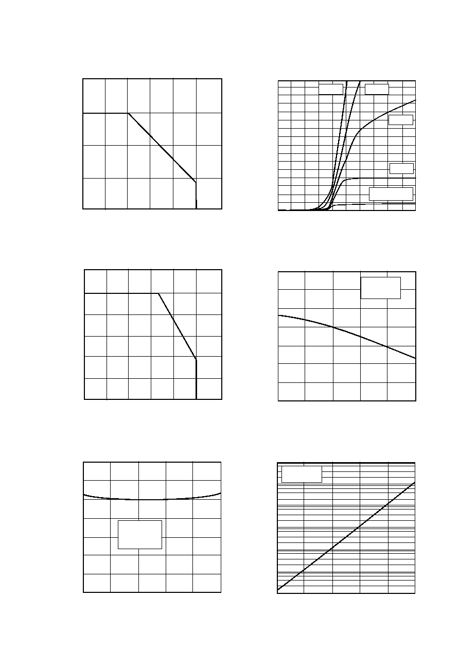
FIGURE 1
100
DB92260m-AAS/A1
7/12/00
0
0.5
1.0
Relative current transfer ratio
Relative Current Transfer Ratio
vs. Ambient Temperature
0 0.4 0.8 1.2 1.6 2.0
40
60
Collector-emitter voltage V
CE
( V )
20
0
-30 0 25 50 75 100
Ambient temperature T
A
( �C )
Collector Current vs. Collector-emitter
Voltage
1.5
-30 0 25 50 75 100
Ambient temperature T
A
( �C )
Collector dark current I
CEO
(A)
Collector Dark Current vs.
Ambient Temperature
V
CE
= 200V
-30 0 25 50 75 100 125
Ambient temperature T
A
( �C )
200
0
Ambient temperature T
A
( �C )
Collector power dissipation P
C
(mW)
60
30
20
10
0
40
50
-30 0 25 50 75 100 125
Collector Power Dissipation vs. Ambient Temperature
Forward Current vs. Ambient Temperature
100
Forward current I
F
(mA)
-30 0 25 50 75 100
Ambient temperature T
A
( �C )
Collector-emitter saturation voltage V
CE(S
A
T)
(V)
Collector-emitter Saturation
Voltage vs. Ambient Temperature
0
0.2
0.4
0.6
0.8
1.0
1.2
I
F
= 20mA
I
C
= 100mA
80
100
120
140
Collector current I
C
(mA)
I
F
= 0.5mA
1mA
2mA
4mA
10mA
I
F
= 1mA
V
CE
= 2V
10
-11
10
-10
10
-9
10
-8
10
-7
10
-6
10
-5
300
400