ISOCOM COMPONENTS LTD
Unit 25B, Park View Road West,
Park View Industrial Estate, Brenda Road
Hartlepool, Cleveland, TS25 1YD
Tel: (01429) 863609 Fax :(01429) 863581
ISOCOM INC
720 E., Park Boulevard, Suite 104,
Plano, TX 75074 USA
Tel: (972) 423-5521
Fax: (972) 422-4549
24/9/97
DB92261-AAS/A2
1mm APERTURE OPTO-ELECTRONIC SINGLE CHANNEL
SLOTTED INTERRUPTER SWITCHES WITH TRANSISTOR
SENSORS AND 450mm FLYING LEADS
ABSOLUTE MAXIMUM RATINGS
(25∞C unless otherwise specified)
Storage Temperature
-40∞C to + 85∞C
Operating Temperature
-25∞C to + 85∞C
Lead Soldering Temperature
(1/16 inch (1.6mm) from case for 10 secs) 260∞C
INPUT DIODE
Forward Current
50mA
Reverse Voltage
5V
Power Dissipation
75mW
OUTPUT TRANSISTOR
Collector-emitter Voltage BV
CEO
30V
Emitter-collector Voltage BV
ECO
5V
Collector Current I
C
20mA
Power Dissipation
75mW
ISTS823A
ISTS824A
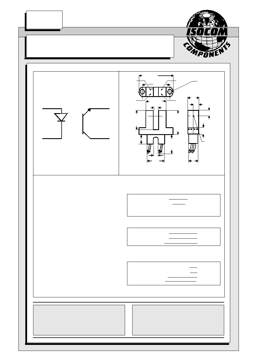
DESCRIPTION
The ISTS823A, ISTS824A opaque
photointerrupters are single channel switches
consisting of a Gallium Arsenide infrared
emitting diode and a NPN silicon photo transistor
mounted in a polycarbonate housing with 450mm
flying leads. The package is designed to optimise
the mechanical resolution, coupling efficiency,
ambient light rejection, cost and reliability.
Operating on the principle that objects opaque to
infrared will interrupt the transmission of light
between an infrared emitting diode and a photo
sensor switching the output from an "ON" state to
an "OFF" state.
FEATURES
l
High Gain
l
3mm Gap between LED and Detector
l
Polycarbonate case protected against
ambient light
APPLICATIONS
l
Copiers, Printers, Facsimilies, Record
Players, Casette Decks, Optoelectronic
Switches
1
2
BLACK
RED
BROWN
ORANGE
25.7
24.1
19.05
Dimensions in mm
1
2
4
3
12.7
3.0
3.3
DIAG 2
PLCS
6.6
3.3
3.0
2.8
3.3
3.0
OPTICAL
CENTRE
LINE
5.6
5.0
11.1
10.5
9.0
8.0
5.5
4.5
3.0
11.1
10.6
450
E

DB92261-AAS/A2
PARAMETER
MIN TYP MAX UNITS TEST CONDITION
Input
Forward Voltage (V
F
)
1.2
1.7
V
I
F
= 50mA
Reverse Voltage (V
R
)
5
V
I
R
= 100
µ
A
Reverse Current (I
R
)
100
µ
A
V
R
= 5V
Output
Collector-emitter Breakdown (BV
CEO
)
30
V
I
C
= 1mA
( Note 1 )
Emitter-collector Breakdown (BV
ECO
)
5
V
I
E
= 100
µ
A
Collector-emitter Dark Current (I
CEO
)
100
nA
V
CE
= 15V
Coupled
On-State Collector Current I
C
(
ON
)
( Note 1 )
ISTS823A
200
µ
A
20mA I
F
, 10V V
CE
ISTS824A
500
µ
A
20mA I
F
, 10V V
CE
Collector-emitter Saturation VoltageV
CE(SAT)
ISTS823A
0.4
V
20mA I
F
, 100
µ
A I
C
ISTS824A
0.4
V
20mA I
F
, 250
µ
A I
C
Turn-on Time
ton
8
µ
s
V
CC
= 5V,
Turn-off Time
toff
50
µ
s
I
F
= 30mA, R
L
= 2.5k
24/9/97
ELECTRICAL CHARACTERISTICS ( T
A
= 25∞C Unless otherwise noted )
Note 1
Special Selections are available on request. Please consult the factory.
DB92261-AAS/A2
24/9/97
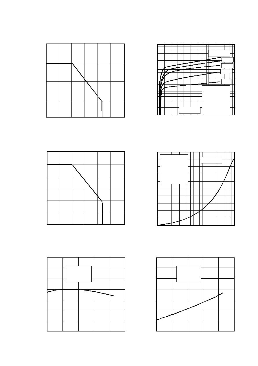
25
-25 0 25 50 75 100 125
Ambient temperature T
A
( ∞C )
75
0
100
Ambient temperature T
A
( ∞C )
Collector power dissipation P
C
(mW)
60
30
20
10
0
40
50
-25 0 25 50 75 100 125
Collector Power Dissipation vs. Ambient Temperature
Forward Current vs. Ambient Temperature
50
Forward current I
F
(mA)
0
0.5
1.0
1.5
I
F
= 20mA
V
CE
= 10V
Ambient temperature T
A
( ∞C )
-25 0 25 50 75 100
-25 0 25 50 75 100
Ambient temperature T
A
( ∞C )
Collector-emitter saturation voltage V
CE(SA
T
)
(V)
Collector-emitter Saturation
Voltage vs. Ambient Temperature
0
0.04
0.08
0.12
0.16
0.20
0.24
0.28
I
F
= 20mA
I
C
= 0.25mA
1 2 5 10 20 50
0
0.4
0.6
0.8
1.0
1.2
0.2
1.4
Normalized output current
Normalized Output Current vs.
Forward Current
Forward current I
F
(mA)
0.1 1 10 100
1
10
Normalized output current
Normalized Output Current vs.
Collector-emitter Voltage
Collector-emitter voltage V
CE
( V )
0.1
0.01
T
A
= 25∞C
0.02
0.04
0.2
0.4
2
4
1.6
1.8
2.0
Normalized to
I
F
= 20mA
V
CE
= 5V
Pulsed
PW = 100
µ
s
PRR = 100pps
I
F
= 50mA
30mA
20mA
5mA
10mA
Normalized Output Current
vs. Ambient Temperature
Normalized output current
Normalized to
I
F
= 20mA
V
CE
= 0.4V
Pulsed
PW = 100
µ
s
PRR = 100pps
T
A
= 25∞C