ISOCOM COMPONENTS LTD
Unit 25B, Park View Road West,
Park View Industrial Estate, Brenda Road
Hartlepool, Cleveland, TS25 1YD
Tel: (01429) 863609 Fax :(01429) 863581
8/7/02
DB92217-AAS/A3
1.2
3.0
4.0
3.0
3.35
7.0
6.0
0.5
0.5
1
2
4
3
2.54
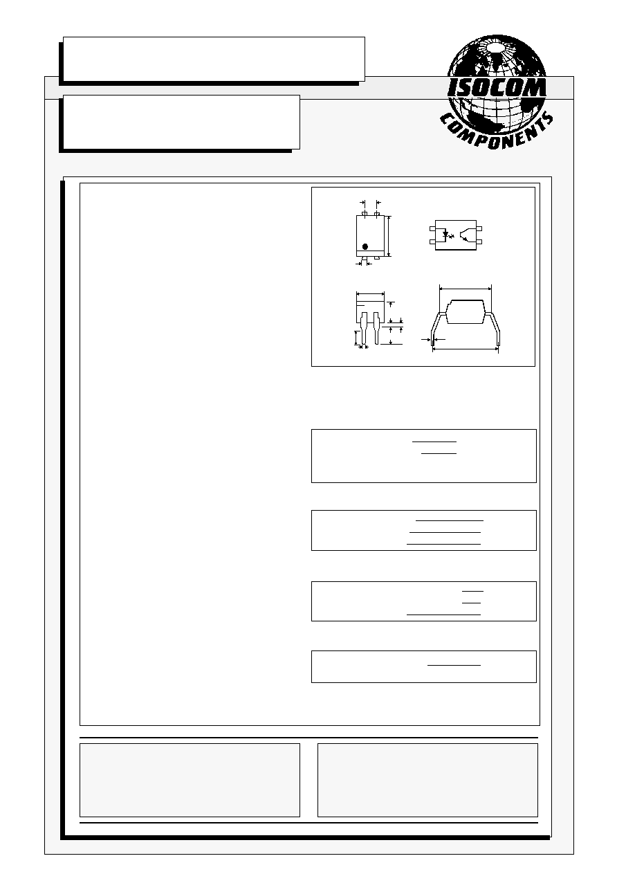
Dimensions in mm
LOW INPUT CURRENT
PHOTOTRANSISTOR
OPTICALLY COUPLED ISOLATORS
APPROVALS
l
UL recognised, File No. E91231
'X' SPECIFICATION APPROVALS
l
VDE 0884
l
l
Certified to EN60950 by the following
Test Bodies :-
Nemko - Certificate No. P01102465
Fimko - Certificate No. FI18162
Semko - Reference No. 0202041/01-25
Demko - Certificate No. 311161-01
DESCRIPTION
The SFH617G series of optically coupled
isolators consist of infrared light emitting diodes
and NPN silicon photo transistors in space
efficient dual in line plastic packages.
FEATURES
l
10mm lead spread
l
Low input current 1mA I
F
l
High Current Transfer Ratios
(40-320% at 10mA, 13% min at 1mA)
l
High Isolation Voltage (5.3kV
RMS
,7.5kV
PK
)
l
High BV
CEO
(70V min)
l
All electrical parameters 100% tested
l
Custom electrical selections available
APPLICATIONS
l
Computer terminals
l
Industrial systems controllers
l
Measuring instruments
l
Signal transmission between systems of
different potentials and impedances
SFH617G-1X, SFH617G-2X, SFH617G-3X, SFH617G-4X
SFH617G-1, SFH617G-2, SFH617G-3, SFH617G-4
ABSOLUTE MAXIMUM RATINGS
(25∞C unless otherwise specified)
Storage Temperature
-55∞C to + 125∞C
Operating Temperature
-30∞C to + 100∞C
Lead Soldering Temperature
(1/16 inch (1.6mm) from case for 10 secs) 260∞C
INPUT DIODE
Forward Current
50mA
Reverse Voltage
6V
Power Dissipation
70mW
OUTPUT TRANSISTOR
Collector-emitter Voltage BV
CEO
70V
Emitter-collector Voltage BV
ECO
6V
Power Dissipation
150mW
POWER DISSIPATION
Total Power Dissipation
200mW
(derate linearly 2.67mW/∞C above 25∞C)
5.08
4.08
10.16
7.62
0.26
ISOCOM INC
1024 S. Greenville Ave, Suite 240,
Allen, TX 75002 USA
Tel: (214) 495-0755 Fax: (214) 495-0901
e-mail info@isocom.com
http://www.isocom.com
DB92217-AAS/A3
8/7/02
PARAMETER
MIN TYP MAX UNITS TEST CONDITION
Input
Forward Voltage (V
F
)
1.65
V
I
F
= 50mA
Reverse Voltage (V
R
)
6
V
I
R
= 10
µ
A
Reverse Current (I
R
)
10
µ
A
V
R
= 6V
Output
Collector-emitter Breakdown (BV
CEO
)
70
V
I
C
= 1mA
( Note 2 )
Emitter-collector Breakdown (BV
ECO
)
6
V
I
E
= 100
µ
A
Collector-emitter Dark Current (I
CEO
)
SFH617G-1,2
50
nA
V
CE
= 10V
SFH617G-3,4
100
nA
Coupled
Current Transfer Ratio (CTR) (Note 2)
SFH617G-1
40
80
%
10mA I
F
, 5V V
CE
SFH617G-2
63
125
%
SFH617G-3
100
200
%
SFH617G-4
160
320
%
SFH617G-1
13
%
1mA I
F
, 5V V
CE
SFH617G-2
22
%
SFH617G-3
34
%
SFH617G-4
56
%
Collector-emitter Saturation Voltage V
CESAT
0.4
V
10mA I
F
, 2.5mA I
C
Input to Output Isolation Voltage V
ISO
5300
V
RMS
See note 1
7500
V
PK
See note 1
Input-output Isolation Resistance R
ISO
5x10
10
V
IO
= 500V (note 1)
ELECTRICAL CHARACTERISTICS ( T
A
= 25∞C Unless otherwise noted )
Note 1
Measured with input leads shorted together and output leads shorted together.
Note 2
Special Selections are available on request. Please consult the factory.
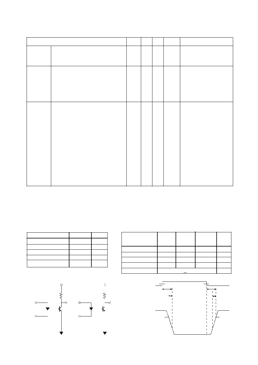
SWITCHING CHARACTERISTICS
1.
Linear Operation
(
without saturation) Fig
1.
I
F
= 10mA, V
CC
= 5V, R
L
= 75
t
on
t
r
t
off
t
f
F
CO
UNITS
2.
Switching Operation (with saturation) Fig 2
V
CC
= 5V, R
L
= 1k
4.2
3.0
23
14
6.0
4.6
25
15
µs
µs
µs
µs
V
UNITS
< 0.4
GROUP
V
CC
= 5.0V
V
CC
= 5.0V
R
L
= 75
R
L
= 1k
OUTPUT
OUTPUT
FIG 2
FIG 1
t
on
t
off
10%
90%
90%
Turn-on Time
Rise Time
Turn-off Time
Fall Time
Cut-off Frequency
µs
µs
µs
µs
kHz
Turn-on Time
Rise Time
Turn-off Time
Fall Time
t
on
t
r
t
off
t
f
V
CESAT
-2 and -3
(I
F
=10mA)
- 4
(I
F
=5mA)
t
r
t
f
INPUT
OUTPUT
10%
-1
(I
F
=20mA)
3.0
2.0
18
11
3.0
2.0
2.3
2.0
250
DB92217-AAS/A3
8/7/02
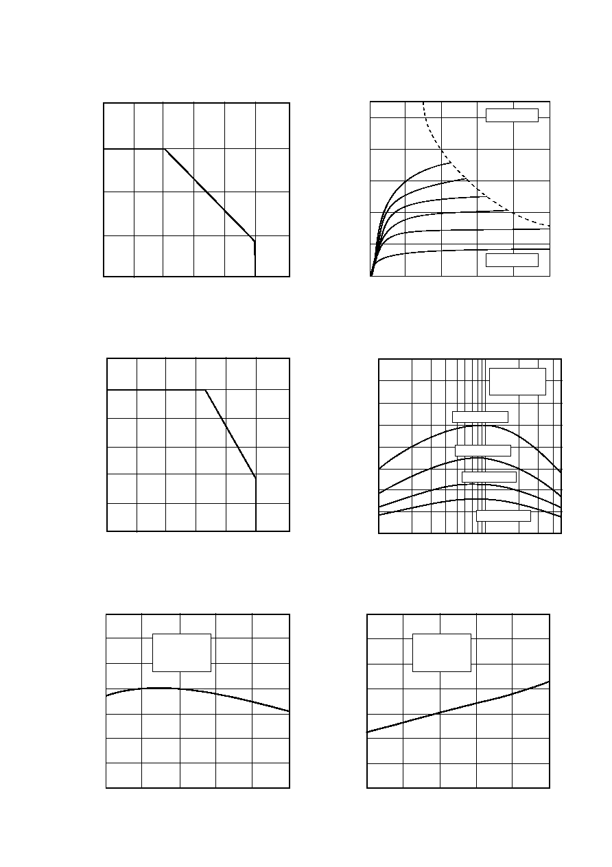
50
Ambient temperature T
A
( ∞C )
150
0
200
Collector power dissipation P
C
(mW)
Collector Power Dissipation vs. Ambient Temperature
-30 0 25 50 75 100
100
0
0.5
1.0
1.5
I
F
= 10mA
V
CE
= 5V
Relative Current Transfer Ratio
vs. Ambient Temperature
Relative current transfer ratio
Collector Current vs. Collector-emitter Voltage
( normalised to SFH617G-3 )
Collector-emitter voltage V
CE
( V )
Collector current I
C
(mA)
0 2 4 6 8 10
0
10
20
30
40
50
T
A
= 25∞C
10
15
20
30
50
-30 0 25 50 75 100 125
-30 0 25 50 75 100
Ambient temperature T
A
( ∞C )
Collector-emitter saturation voltage V
CE(S
A
T)
(V)
Collector-emitter Saturation
Voltage vs. Ambient Temperature
0
0.04
0.08
0.12
0.16
0.20
0.24
0.28
I
F
= 10mA
I
C
= 2.5mA
Ambient temperature T
A
( ∞C )
I
F
= 5mA
0
80
120
160
200
240
40
280
320
Forward current I
F
(mA)
Current Transfer Ratio vs. Forward Current
Current transfer ratio CTR (%)
V
CE
= 5V
T
A
= 25∞C
1 2 5 10 20 50
SFH617G-2
SFH617G-3
SFH617G-4
Ambient temperature T
A
( ∞C )
60
30
20
10
0
40
50
-30 0 25 50 75 100 125
Forward Current vs. Ambient Temperature
Forward current I
F
(mA)
SFH617G-1