ISOCOM COMPONENTS LTD
Unit 25B, Park View Road West,
Park View Industrial Estate, Brenda Road
Hartlepool, Cleveland, TS25 1YD
Tel: (01429) 863609 Fax :(01429) 863581
7/12/00
0.26
20.32
19.32
3.35
4.0
3.0
0.5
7.62
13∞
Max
7.0
6.0
2.54
1.2
0.5
3.0
1.2
3.0
4.0
3.0
3.35
7.0
6.0
0.5
0.5
7.62
1
2
4
3
0.26
13∞
Max
2.54
10.16
0.26
OPTION G
7.62
3.0
10.16
9.16
3.35
7.0
6.0
7.62
1.2
13∞
Max
0.5
0.26
2.54
1
2
3
7
8
15
10
9
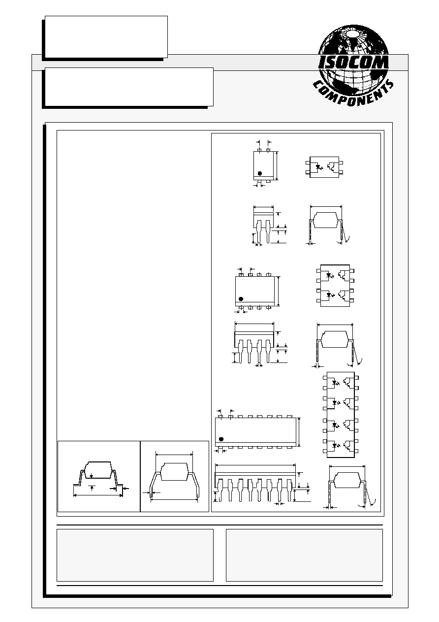
HIGH DENSITY MOUNTING
PHOTODARLINGTON OPTICALLY
COUPLED ISOLATORS
DESCRIPTION
The TIL197, TIL198, TIL199 series of
optically coupled isolators consist of infrared
light emitting diodes and NPN silicon photo
darlingtons in space efficient dual in line plastic
packages. The standard parts TIL197, TIL198,
TIL199 are tested for a CTR of 500% minimum.
Parts with the suffix A or B are tested for a CTR
of 1000 and 1500% minimum respectively.
FEATURES
l
Options :-
10mm lead spread - add G after part no.
Surface mount - add SM after part no.
Tape&reel - add SMT&R after part no.
l
High Current Transfer Ratio (500%min)
l
High Isolation Voltage (5.3kV
RMS
,7.5kV
PK
)
l
All electrical parameters 100% tested
l
Custom electrical selections available
APPLICATIONS
l
Computer terminals
l
Industrial systems controllers
l
Measuring instruments
l
Signal transmission between systems of
different potentials and impedances
OPTION SM
SURFACE MOUNT
Dimensions in mm
5.08
4.08
1
2
3
4
8
4.0
3.0
0.5
16
4
13
6
11
5
12
14
6
5
7
TIL197,TIL198, TIL199
TIL197A, TIL198A, TIL199A
TIL197B, TIL198B, TIL199B
TIL197
TIL197A
TIL197B
TIL198
TIL198A
TIL198B
TIL199
TIL199A
TIL199B
APPROVALS
l
UL recognised, File No. E91231
'X' SPECIFICATION APPROVALS
l
VDE 0884 approval pending
l
Certified to EN60950 by the following
Test Bodies :-
Nemko - Certificate No. P96102022
Fimko - Registration No. 192313-01..25
Semko - Reference No. 9639052 01
Demko - Reference No. 305969
ISOCOM INC
1024 S. Greenville Ave, Suite 240,
Allen, TX 75002 USA
Tel: (214) 495-0755 Fax: (214) 495-0901
e-mail info@isocom.com
http://www.isocom.com
10.46
9.86
0.6
0.1
1.25
0.75
DB92416m-AAS/A2
DB92416m-AAS/A2
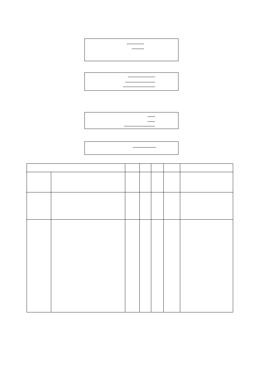
PARAMETER
MIN TYP MAX UNITS TEST CONDITION
Input
Forward Voltage (V
F
)
1.2
1.4
V
I
F
= 20mA
Reverse Voltage (V
R
)
5
V
I
R
= 10
µ
A
Reverse Current (I
R
)
10
µ
A
V
R
= 5V
Output
Collector-emitter Breakdown (BV
CEO
)
35
V
I
C
= 0.5mA
( Note 2 )
Emitter-collector Breakdown (BV
ECO
)
6
V
I
E
= 100
µ
A
Collector-emitter Dark Current (I
CEO
)
100
nA
V
CE
= 10V
Coupled
Current Transfer Ratio (CTR) (Note 2
)
TIL197, TIL198, TIL199
500
7500
2mA I
F
, 1V V
CE
TIL197A, TIL198A, TIL199A
1000
7500
2mA I
F
, 1V V
CE
TIL197B, TIL198B, TIL199B
1500
7500
2mA I
F
, 1V V
CE
Collector-emitter Saturation VoltageV
CE
(SAT)
0.8
1.0
V
2mA I
F
, 10mA I
C
Input to Output Isolation Voltage V
ISO
5300
V
RMS
See note 1
7500
V
PK
See note 1
Input-output Isolation Resistance R
ISO
5x10
10
V
IO
= 500V (note 1)
Output Rise Time
tr
100
µ
s
V
CC
= 10V ,
Output Fall Time
tf
100
µ
s
I
C
= 10mA, R
L
= 100
7/12/00
ELECTRICAL CHARACTERISTICS ( T
A
= 25∞C Unless otherwise noted )
Note 1
Measured with input leads shorted together and output leads shorted together.
Note 2
Special Selections are available on request. Please consult the factory.
ABSOLUTE MAXIMUM RATINGS
(25∞C unless otherwise specified)
Storage Temperature
-55∞C to + 125∞C
Operating Temperature
-55∞C to + 100∞C
Lead Soldering Temperature
(1/16 inch (1.6mm) from case for 10 secs) 260∞C
INPUT DIODE
Forward Current
50mA
Reverse Voltage
6V
Power Dissipation
70mW
OUTPUT TRANSISTOR
Collector-emitter Voltage BV
CEO
35V
Emitter-collector Voltage BV
ECO
6V
Power Dissipation
150mW
POWER DISSIPATION
Total Power Dissipation
200mW
(derate linearly 2.67mW/∞C above 25∞C)
DB92416m-AAS/A2
7/12/00
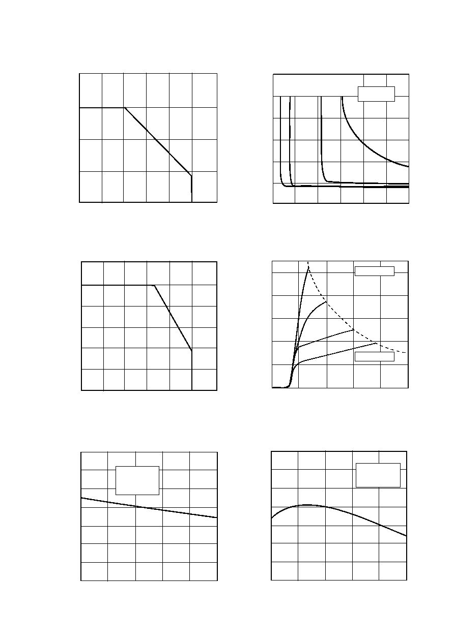
50
-30 0 25 50 75 100 125
Ambient temperature T
A
( ∞C )
150
0
200
Ambient temperature T
A
( ∞C )
Collector power dissipation P
C
(mW)
60
30
20
10
0
40
50
-30 0 25 50 75 100 125
Collector Power Dissipation vs. Ambient Temperature
Forward Current vs. Ambient Temperature
-30 0 25 50 75 100
Ambient temperature T
A
( ∞C )
Collector-emitter saturation voltage V
CE(S
A
T)
(V)
Collector-emitter Saturation
Voltage vs. Ambient Temperature
100
0
0.2
0.4
0.6
0.8
1.0
1.2
Forward current I
F
(mA)
I
F
= 2mA
I
C
= 10mA
T
A
= 25∞C
0
1
2
3
4
5
Collector-emitter Saturation
Voltage vs. Forward Current
Forward current I
F
(mA)
Collector-emitter saturation voltage V
CE(S
A
T)
(V)
Ic
=1mA
5mA
30mA
50mA
6
0
0.5
1.0
1.5
Relative Current Transfer Ratio
vs. Ambient Temperature
Relative current transfer ratio
I
F
= 2mA
V
CE
= 1V
-30 0 25 50 75 100
Ambient temperature T
A
( ∞C )
0 0.5 1.0 1.5 2.0 2.5 3.0
Collector Current vs. Collector-emitter Voltage
Collector-emitter voltage V
CE
( V )
Collector current I
C
(mA)
0 1 2 3 4 5
0
20
40
60
80
100
T
A
= 25∞C
2mA
5mA
10mA
I
F
= 1mA