 | –≠–ª–µ–∫—Ç—Ä–æ–Ω–Ω—ã–π –∫–æ–º–ø–æ–Ω–µ–Ω—Ç: 42S16800A | –°–∫–∞—á–∞—Ç—å:  PDF PDF  ZIP ZIP |

Integrated Silicon Solution, Inc. -- www.issi.com --
1-800-379-4774
1
PRELIMINARY INFORMATION, Rev. 00C
01/20/05
Copyright © 2005 Integrated Silicon Solution, Inc. All rights reserved. ISSI reserves the right to make changes to this specification and its products at any
time without notice. ISSI assumes no liability arising out of the application or use of any information, products or services described herein. Customers are
advised to obtain the latest version of this device specification before relying on any published information and before placing orders for products.
IS42S81600A,
IS42S16800A,
IS42S32400A,
ISSI
Æ
FEATURES
∑ Clock frequency: 166,143,100 MHz
∑ Fully synchronous; all signals referenced to a
positive clock edge
∑ Internal bank for hiding row access/precharge
∑ Power supply
V
DD
V
DDQ
IS42S81600A
3.3V
3.3V
IS42S16800A
3.3V
3.3V
IS42S32400A
3.3V
3.3V
∑ LVTTL interface
∑ Programmable burst length
≠ (1, 2, 4, 8, full page)
∑ Programmable burst sequence:
Sequential/Interleave
∑ Auto Refresh (CBR)
∑ Self Refresh with programmable refresh periods
∑ 4096 refresh cycles every 64 ms
∑ Random column address every clock cycle
∑ Programmable
CAS
latency (2, 3 clocks)
∑ Burst read/write and burst read/single write
operations capability
∑ Burst termination by burst stop and precharge
command
∑ Industrial Temperature Availability
∑ Lead-free Availability
OVERVIEW
ISSI
's 128Mb Synchronous DRAM achieves high-speed
data transfer using pipeline architecture. All inputs and
outputs signals refer to the rising edge of the clock
input.The 128Mb SDRAM is organized as follows.
16Meg x 8, 8Meg x16 & 4Meg x 32
128-MBIT SYNCHRONOUS DRAM
PRELIMINARY INFORMATION
JANUARY 2005
KEY TIMING PARAMETERS
Parameter
-6
-7
-10
Unit
Clk Cycle Time
CAS
Latency = 3
6
7
10
ns
CAS
Latency = 2
-
10
10
ns
Clk Frequency
CAS
Latency = 3
166
143
100
Mhz
CAS
Latency = 2
-
100
100
Mhz
Access Time from Clock
CAS
Latency = 3
5.4
5.4
7
ns
CAS
Latency = 2
-
6
9
ns
IS42S81600A
IS42S16800A
IS42S32400A
4M x8x4 Banks
2M x16x4 Banks
1M x32x4 Banks
54-pin TSOPII
54-pin TSOPII
86-pin TSOPII
ISSI
Æ
2
Integrated Silicon Solution, Inc. -- www.issi.com --
1-800-379-4774
PRELIMINARY INFORMATION
Rev. 00C
01/20/05
IS42S81600A, IS42S16800A, IS42S32400A
DEVICE OVERVIEW
The 128Mb SDRAM is a high speed CMOS, dynamic
random-access memory designed to operate in 3.3V V
DD
and 3.3V V
DDQ
memory systems containing 134,217,728
bits. Internally configured as a quad-bank DRAM with a
synchronous interface. Each 33,554,432-bit bank is orga-
nized as 4,096 rows by 512 columns by 16 bits.
The 128Mb SDRAM includes an AUTO REFRESH MODE,
and a power-saving, power-down mode. All signals are
registered on the positive edge of the clock signal, CLK. All
inputs and outputs are LVTTL compatible.
The 128Mb SDRAM has the ability to synchronously burst
data at a high data rate with automatic column-address
generation, the ability to interleave between internal banks
to hide precharge time and the capability to randomly
change column addresses on each clock cycle during
burst access.
A self-timed row precharge initiated at the end of the burst
sequence is available with the AUTO PRECHARGE func-
tion enabled. Precharge one bank while accessing one of the
other three banks will hide the precharge cycles and provide
seamless, high-speed, random-access operation.
SDRAM read and write accesses are burst oriented starting at
a selected location and continuing for a programmed num-
ber of locations in a programmed sequence. The registra-
tion of an ACTIVE command begins accesses, followed by
a READ or WRITE command. The ACTIVE command in
conjunction with address bits registered are used to select
the bank and row to be accessed (BA0, BA1 select the
bank; A0-A11 select the row). The READ or WRITE
commands in conjunction with address bits registered are
used to select the starting column location for the burst
access.
Programmable READ or WRITE burst lengths consist of 1,
2, 4 and 8 locations or full page, with a burst terminate
option.
CLK
CKE
CS
RAS
CAS
WE
A9
A8
A7
A6
A5
A4
A3
A2
A1
A0
BA0
BA1
A10
COMMAND
DECODER
&
CLOCK
GENERATOR
MODE
REGISTER
REFRESH
CONTROLLER
REFRESH
COUNTER
SELF
REFRESH
CONTROLLER
ROW
ADDRESS
LATCH
MUL
TIPLEXER
COLUMN
ADDRESS LATCH
BURST COUNTER
COLUMN
ADDRESS BUFFER
COLUMN DECODER
DATA IN
BUFFER
DATA OUT
BUFFER
DQML
DQMH
I/O 0-15
V
DD
/V
DDQ
Vss/Vss
Q
12
12
9
12
12
9
16
16
16
16
512
(x 16)
4096
4096
4096
R
O
W DECODER
4096
MEMORY CELL
ARRAY
BANK 0
SENSE AMP I/O GATE
BANK CONTROL LOGIC
ROW
ADDRESS
BUFFER
A11
2
FUNCTIONAL BLOCK DIAGRAM (FOR 2MX16X4 BANKS ONLY)
Integrated Silicon Solution, Inc. -- www.issi.com --
1-800-379-4774
3
PRELIMINARY INFORMATION
Rev. 00C
01/20/05
ISSI
Æ
IS42S81600A, IS42S16800A, IS42S32400A
V
DD
I/O0
V
DD
Q
NC
I/O1
V
SS
Q
NC
I/O2
V
DD
Q
NC
I/O3
V
SS
Q
NC
V
DD
NC
WE
CAS
RAS
CS
BA0
BA1
A10
A0
A1
A2
A3
V
DD
1
2
3
4
5
6
7
8
9
10
11
12
13
14
15
16
17
18
19
20
21
22
23
24
25
26
27
54
53
52
51
50
49
48
47
46
45
44
43
42
41
40
39
38
37
36
35
34
33
32
31
30
29
28
V
SS
I/O7
V
SS
Q
NC
I/O6
V
DD
Q
NC
I/O5
V
SS
Q
NC
I/O4
V
DD
Q
NC
V
SS
NC
DQM
CLK
CKE
NC
A11
A9
A8
A7
A6
A5
A4
V
SS
PIN CONFIGURATIONS
54 pin TSOP - Type II for x8
PIN DESCRIPTIONS
A0-A11
Row Address Input
A0-A9
Column Address Input
BA0, BA1
Bank Select Address
I/O0 to I/O7
Data I/O
CLK
System Clock Input
CKE
Clock Enable
CS
Chip Select
RAS
Row Address Strobe Command
CAS
Column Address Strobe Command
WE
Write Enable
DQM
x 8 Lower Byte, Input/Output Mask
V
DD
Power
Vss
Ground
V
DDQ
Power Supply for I/O Pin
Vss
Q
Ground for I/O Pin
NC
No Connection
ISSI
Æ
4
Integrated Silicon Solution, Inc. -- www.issi.com --
1-800-379-4774
PRELIMINARY INFORMATION
Rev. 00C
01/20/05
IS42S81600A, IS42S16800A, IS42S32400A
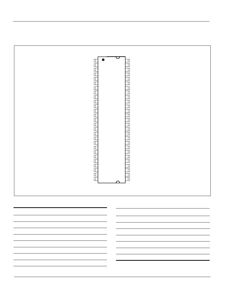
PIN CONFIGURATIONS
54 pin TSOP - Type II for x16
PIN DESCRIPTIONS
A0-A11
Row Address Input
A0-A8
Column Address Input
BA0, BA1
Bank Select Address
I/O0 to I/O15
Data I/O
CLK
System Clock Input
CKE
Clock Enable
CS
Chip Select
RAS
Row Address Strobe Command
CAS
Column Address Strobe Command
V
DD
I/O0
V
DD
Q
I/O1
I/O2
V
SS
Q
I/O3
I/O4
V
DD
Q
I/O5
I/O6
V
SS
Q
I/O7
V
DD
LDQM
WE
CAS
RAS
CS
BA0
BA1
A10
A0
A1
A2
A3
V
DD
1
2
3
4
5
6
7
8
9
10
11
12
13
14
15
16
17
18
19
20
21
22
23
24
25
26
27
54
53
52
51
50
49
48
47
46
45
44
43
42
41
40
39
38
37
36
35
34
33
32
31
30
29
28
V
SS
I/O15
V
SS
Q
I/O14
I/O13
V
DD
Q
I/O12
I/O11
V
SS
Q
I/O10
I/O9
V
DD
Q
I/O8
V
SS
NC
UDQM
CLK
CKE
NC
A11
A9
A8
A7
A6
A5
A4
V
SS
WE
Write Enable
DQML
x16 Lower Byte, Input/Output Mask
DQMH
x16 Upper Byte, Input/Output Mask
V
DD
Power
Vss
Ground
V
DDQ
Power Supply for I/O Pin
Vss
Q
Ground for I/O Pin
NC
No Connection
Integrated Silicon Solution, Inc. -- www.issi.com --
1-800-379-4774
5
PRELIMINARY INFORMATION
Rev. 00C
01/20/05
ISSI
Æ
IS42S81600A, IS42S16800A, IS42S32400A
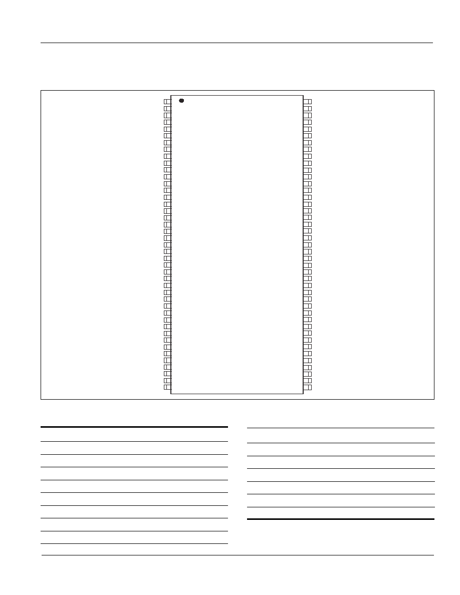
PIN CONFIGURATIONS
86 pin TSOP - Type II for x32
PIN DESCRIPTIONS
A0-A11
Row Address Input
A0-A7
Column Address Input
BA0, BA1
Bank Select Address
I/O0 to I/O31
Data I/O
CLK
System Clock Input
CKE
Clock Enable
CS
Chip Select
RAS
Row Address Strobe Command
CAS
Column Address Strobe Command
V
DD
I/O0
V
DD
Q
I/O1
I/O2
V
SS
Q
I/O3
I/O4
V
DD
Q
I/O5
I/O6
V
SS
Q
I/O7
NC
V
DD
DQM0
WE
CAS
RAS
CS
A11
BA0
BA1
A10
A0
A1
A2
DQM2
V
DD
NC
I/O16
V
SS
Q
I/O17
I/O18
V
DD
Q
I/O19
I/O20
V
SS
Q
I/O21
I/O22
V
DD
Q
I/O23
V
DD
1
2
3
4
5
6
7
8
9
10
11
12
13
14
15
16
17
18
19
20
21
22
23
24
25
26
27
28
29
30
31
32
33
34
35
36
37
38
39
40
41
42
43
86
85
84
83
82
81
80
79
78
77
76
75
74
73
72
71
70
69
68
67
66
65
64
63
62
61
60
59
58
57
56
55
54
53
52
51
50
49
48
47
46
45
44
V
SS
I/O15
V
SS
Q
I/O14
I/O13
V
DD
Q
I/O12
I/O11
V
SS
Q
I/O10
I/O9
V
DD
Q
I/O8
NC
V
SS
DQM1
NC
NC
CLK
CKE
A9
A8
A7
A6
A5
A4
A3
DQM3
V
SS
NC
I/O31
V
DD
Q
I/O30
I/O29
V
SS
Q
I/O28
I/O27
V
DD
Q
I/O26
I/O25
V
SS
Q
I/O24
V
SS
WE
Write Enable
DQM0-DQM3
x32 Input/Output Mask
V
DD
Power
Vss
Ground
V
DDQ
Power Supply for I/O Pin
Vss
Q
Ground for I/O Pin
NC
No Connection