 | –≠–ª–µ–∫—Ç—Ä–æ–Ω–Ω—ã–π –∫–æ–º–ø–æ–Ω–µ–Ω—Ç: 42S32200 | –°–∫–∞—á–∞—Ç—å:  PDF PDF  ZIP ZIP |

Integrated Silicon Solution, Inc. -- 1-800-379-4774
1
P R E L I M I N A R Y I N F O R M A T I O N
R e v . 0 0 B
08/14/03
IS42S32200
ISSI
Æ
Copyright © 2003 Integrated Silicon Solution, Inc. All rights reserved. ISSI reserves the right to make changes to this specification and its products at any time
without notice. ISSI assumes no liability arising out of the application or use of any information, products or services described herein. Customers are advised to
obtain the latest version of this device specification before relying on any published information and before placing orders for products.
FEATURES
∑ Clock frequency: 166, 143 MHz
∑ Fully synchronous; all signals referenced to a
positive clock edge
∑ Internal bank for hiding row access/precharge
∑ Single 3.3V power supply
∑ LVTTL interface
∑ Programmable burst length
≠ (1, 2, 4, 8, full page)
∑ Programmable burst sequence:
Sequential/Interleave
∑ Self refresh modes
∑ 4096 refresh cycles every 64 ms
∑ Random column address every clock cycle
∑ Programmable
CAS latency (2, 3 clocks)
∑ Burst read/write and burst read/single write
operations capability
∑ Burst termination by burst stop and precharge
command
∑ Industrial temperature availability
∑ Package 400-mil 86-pin TSOP II
OVERVIEW
ISSI
's 64Mb Synchronous DRAM IS42S32200 is organized
as 524,288 bits x 32-bit x 4-bank for improved performance.
The synchronous DRAMs achieve high-speed data transfer
using pipeline architecture. All inputs and outputs signals
refer to the rising edge of the clock input.
512K Bits x 32 Bits x 4 Banks (64-MBIT)
SYNCHRONOUS DYNAMIC RAM
PRELIMINARY INFORMATION
August 2003
PIN CONFIGURATION
(86-Pin TSOP (Type II)
VCC
I/O0
VCCQ
I/O1
I/O2
GNDQ
I/O3
I/O4
VCCQ
I/O5
I/O6
GNDQ
I/O7
NC
VCC
DQM0
WE
CAS
RAS
CS
NC
BA0
BA1
A10/AP
A0
A1
A2
DQM2
VCC
NC
I/O16
GNDQ
I/O17
I/O18
VCCQ
I/O19
I/O20
GNDQ
I/O21
I/O22
VCCQ
I/O23
VCC
1
2
3
4
5
6
7
8
9
10
11
12
13
14
15
16
17
18
19
20
21
22
23
24
25
26
27
28
29
30
31
32
33
34
35
36
37
38
39
40
41
42
43
86
85
84
83
82
81
80
79
78
77
76
75
74
73
72
71
70
69
68
67
66
65
64
63
62
61
60
59
58
57
56
55
54
53
52
51
50
49
48
47
46
45
44
GND
I/O15
GNDQ
I/O14
I/O13
VCCQ
I/O12
I/O11
GNDQ
I/O10
I/O9
VCCQ
I/O8
NC
GND
DQM1
NC
NC
CLK
CKE
A9
A8
A7
A6
A5
A4
A3
DQM3
GND
NC
I/O31
VCCQ
I/O30
I/O29
GNDQ
I/O28
I/O27
VCCQ
I/O26
I/O25
GNDQ
I/O24
GND
PIN DESCRIPTIONS
A0-A10
Address Input
BA0, BA1
Bank Select Address
I/O0 to I/O31
Data I/O
CLK
System Clock Input
CKE
Clock Enable
CS
Chip Select
RAS
Row Address Strobe Command
CAS
Column Address Strobe Command
WE
Write Enable
DQM0 to DQM3 Input/Output Mask
Vcc
Power
GND
Ground
Vcc
Q
Power Supply for I/O Pin
GND
Q
Ground for I/O Pin
NC
No Connection
IS42S32200
ISSI
Æ
2
Integrated Silicon Solution, Inc. -- 1-800-379-4774
A D V A N C E I N F O R M A T I O N
R e v . 0 0 B
08/14/03
GENERAL DESCRIPTION
The 64Mb SDRAM is a high speed CMOS, dynamic
random-access memory designed to operate in 3.3V
memory systems containing 67,108,864 bits. Internally
configured as a quad-bank DRAM with a synchronous
interface. Each 16,777,216-bit bank is organized as 2,048
rows by 256 columns by 32 bits.
The 64Mb SDRAM includes an AUTO REFRESH MODE,
and a power-saving, power-down mode. All signals are
registered on the positive edge of the clock signal, CLK.
All inputs and outputs are LVTTL compatible.
The 64Mb SDRAM has the ability to synchronously burst
data at a high data rate with automatic column-address
generation, the ability to interleave between internal banks
to hide precharge time and the capability to randomly
change column addresses on each clock cycle during
burst access.
A self-timed row precharge initiated at the end of the burst
sequence is available with the AUTO PRECHARGE
function enabled. Precharge one bank while accessing one
of the other three banks will hide the precharge cycles and
provide seamless, high-speed, random-access operation.
SDRAM read and write accesses are burst oriented starting
at a selected location and continuing for a programmed
number of locations in a programmed sequence. The
registration of an ACTIVE command begins accesses,
followed by a READ or WRITE command. The ACTIVE
command in conjunction with address bits registered are
used to select the bank and row to be accessed (BA0, BA1
select the bank; A0-A10 select the row). The READ or
WRITE commands in conjunction with address bits reg-
istered are used to select the starting column location for
the burst access.
Programmable READ or WRITE burst lengths consist of
1, 2, 4 and 8 locations or full page, with a burst terminate
option.
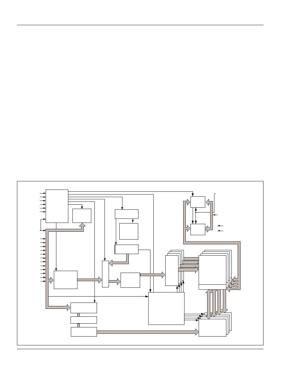
FUNCTIONAL BLOCK DIAGRAM
CLK
CKE
CS
RAS
CAS
WE
A9
A8
A7
A6
A5
A4
A3
A2
A1
A0
BA0
BA1
A10
COMMAND
DECODER
&
CLOCK
GENERATOR
MODE
REGISTER
REFRESH
CONTROLLER
REFRESH
COUNTER
SELF
REFRESH
CONTROLLER
ROW
ADDRESS
LATCH
MUL
TIPLEXER
COLUMN
ADDRESS LATCH
BURST COUNTER
COLUMN
ADDRESS BUFFER
COLUMN DECODER
DATA IN
BUFFER
DATA OUT
BUFFER
DQM0-3
I/O 0-31
Vcc/Vcc
Q
GND/GNDQ
10
10
10
10
32
32
32
32
256
(x 32)
2048
2048
2048
R
O
W DECODER
2048
MEMORY CELL
ARRAY
BANK 0
SENSE AMP I/O GATE
BANK CONTROL LOGIC
ROW
ADDRESS
BUFFER

IS42S32200
ISSI
Æ
Integrated Silicon Solution, Inc. -- 1-800-379-4774
3
A D V A N C E I N F O R M A T I O N
R e v . 0 0 B
08/14/03
PIN FUNCTIONS
Symbol
Pin No.
Type
Function (In Detail)
A0-A10
25 to 27
Input Pin
Address Inputs: A0-A10 are sampled during the ACTIVE
60 to 66
command (row-address A0-A10) and READ/WRITE command (A0-A7
24
with A10 defining auto precharge) to select one location out of the memory array
in the respective bank. A10 is sampled during a PRECHARGE command to
determine if all banks are to be precharged (A10 HIGH) or bank selected by
BA0, BA1 (LOW). The address inputs also provide the op-code during a LOAD
MODE REGISTER command.
BA0, BA1
22,23
Input Pin
Bank Select Address: BA0 and BA1 defines which bank the ACTIVE, READ,
WRITE or PRECHARGE command is being applied.
CAS
18
Input Pin
CAS, in conjunction with the RAS and WE, forms the device command. See the
"Command Truth Table" for details on device commands.
CKE
67
Input Pin
The CKE input determines whether the CLK input is enabled. The next rising edge
of the CLK signal will be valid when is CKE HIGH and invalid when LOW. When
CKE is LOW, the device will be in either power-down mode, clock suspend mode,
or self refresh mode. CKE is an asynchronous input.
CLK
68
Input Pin
CLK is the master clock input for this device. Except for CKE, all inputs to this
device are acquired in synchronization with the rising edge of this pin.
CS
20
Input Pin
The
CS input determines whether command input is enabled within the device.
Command input is enabled when
CS is LOW, and disabled with CS is HIGH. The
device remains in the previous state when
CS is HIGH.
I/O0 to
2, 4, 5, 7, 8, 10,11,13
I/O Pin
I/O0 to I/O15 are I/O pins. I/O through these pins can be controlled in byte units
I/O31
74,76,77,79,80,82,83,85
using the DQM0-DQM3 pins
45,47,48,50,51,53,54,56
31,33,34,36,37,39,40,42
DQM0
16,28,59,71
Input Pin
DQMx control thel ower and upper bytes of the I/O buffers. In read mode,
DQM3
the output buffers are place in a High-Z state. During a WRITE cycle the input data
is masked. When DQMx is sampled HIGH and is an input mask signal for write
accesses and an output enable signal for read accesses. I/O0 through I/O7 are
controlled by DQM0. I/O8 throughI/O15 are controlled by DQM1. I/O16 through I/
O23 are controlled by DQM2. I/O24 through I/O31 are controlled by DQM3.
RAS
19
Input Pin
RAS, in conjunction with CAS and WE, forms the device command. See the
"Command Truth Table" item for details on device commands.
WE
17
Input Pin
WE, in conjunction with RAS and CAS, forms the device command. See the
"Command Truth Table" item for details on device commands.
V
CCQ
3,9,35,41,49,55,25,81
Supply Pin
V
CCQ
is the output buffer power supply.
V
CC
1,15,29,43
Supply Pin
V
CC
is the device internal power supply.
GND
Q
6,12,32,38,46,52,78,84
Supply Pin
GND
Q
is the output buffer ground.
GND
44,58,72,86
Supply Pin
GND is the device internal ground.

IS42S32200
ISSI
Æ
4
Integrated Silicon Solution, Inc. -- 1-800-379-4774
A D V A N C E I N F O R M A T I O N
R e v . 0 0 B
08/14/03
FUNCTION (In Detail)
A0-A10 are address inputs sampled during the ACTIVE
(row-address A0-A10) and READ/WRITE command (A0-A7
with A10 defining auto PRECHARGE). A10 is sampled during
a PRECHARGE command to determine if all banks are to
be PRECHARGED (A10 HIGH) or bank selected by BA0,
BA1 (LOW). The address inputs also provide the op-code
during a LOAD MODE REGISTER command.
Bank Select Address (BA0 and BA1) defines which bank the
ACTIVE, READ, WRITE or PRECHARGE command is
being applied.
CAS, in conjunction with the RAS and WE, forms the
device command. See the "Command Truth Table" for
details on device commands.
The CKE input determines whether the CLK input is
enabled. The next rising edge of the CLK signal will be
valid when is CKE HIGH and invalid when LOW. When
CKE is LOW, the device will be in either power-down
mode, CLOCK SUSPEND mode, or SELF-REFRESH
mode. CKE is an asynchronous input.
CLK is the master clock input for this device. Except for
CKE, all inputs to this device are acquired in synchroni-
zation with the rising edge of this pin.
The CS input determines whether command input is
enabled within the device. Command input is enabled
when CS is LOW, and disabled with CS is HIGH. The
device remains in the previous state when CS is HIGH. I
I/O0 through I/O7 are controlled by DQM0. I/O8 through
I/O15 are controlled by DQM1. I/O16 through I/O23 are
controlled by DQM2. I/O24 through I/O31 are controlled
by DQM3. In read mode, DQMx control the output buffer.
When DQMx is LOW, the corresponding buffer byte is
enabled, and when HIGH, disabled. The outputs go to the
HIGH Impedance State when DQMx is HIGH. This func-
tion corresponds to OE in conventional DRAMs. In write
mode, DQMx control the input buffer. When DQMx is
LOW, the corresponding buffer byte is enabled, and data
can be written to the device. When DQMx is HIGH, input
data is masked and cannot be written to the device.
RAS, in conjunction with CAS and WE , forms the device
command. See the "Command Truth Table" item for
details on device commands.
WE , in conjunction with RAS and CAS , forms the device
command. See the "Command Truth Table" item for
details on device commands.
V
CCQ
is the output buffer power supply.
V
CC
is the device internal power supply.
GND
Q
is the output buffer ground.
GND is the device internal ground.
READ
The READ command selects the bank from BA0, BA1
inputs and starts a burst read access to an active row.
Inputs A0-A7 provides the starting column location. When
A10 is HIGH, this command functions as an AUTO
PRECHARGE command. When the auto precharge is
selected, the row being accessed will be precharged at
the end of the READ burst. The row will remain open for
subsequent accesses when AUTO PRECHARGE is not
selected. DQ's read data is subject to the logic level on
the DQM inputs two clocks earlier. When a given DQM
signal was registered HIGH, the corresponding DQ's will
be High-Z two clocks later. DQ's will provide valid data
when the DQM signal was registered LOW.
WRITE
A burst write access to an active row is initiated with the
WRITE command. BA0, BA1 inputs selects the bank, and
the starting column location is provided by inputs A0-A7.
Whether or not AUTO-PRECHARGE is used is deter-
mined by A10.
The row being accessed will be precharged at the end of
the WRITE burst, if AUTO PRECHARGE is selected. If
AUTO PRECHARGE is not selected, the row will remain
open for subsequent accesses.
A memory array is written with corresponding input data
on DQ's and DQM input logic level appearing at the same
time. Data will be written to memory when DQM signal is
LOW. When DQM is HIGH, the corresponding data inputs
will be ignored, and a WRITE will not be executed to that
byte/column location.
PRECHARGE
The PRECHARGE command is used to deactivate the
open row in a particular bank or the open row in all banks.
BA0, BA1 can be used to select which bank is precharged
or they are treated as "Don't Care". A10 determined
whether one or all banks are precharged. After executing
this command, the next command for the selected banks(s)
is executed after passage of the period t
RP
, which is the
period required for bank precharging. Once a bank has
been precharged, it is in the idle state and must be
activated prior to any READ or WRITE commands being
issued to that bank.
AUTO PRECHARGE
The AUTO PRECHARGE function ensures that the
precharge is initiated at the earliest valid stage within a
burst. This function allows for individual-bank precharge
without requiring an explicit command. A10 to enables the
AUTO PRECHARGE function in conjunction with a spe-
cific READ or WRITE command. For each individual
READ or WRITE command, auto precharge is either

IS42S32200
ISSI
Æ
Integrated Silicon Solution, Inc. -- 1-800-379-4774
5
A D V A N C E I N F O R M A T I O N
R e v . 0 0 B
08/14/03
enabled or disabled. AUTO PRECHARGE does not apply
except in full-page burst mode. Upon completion of the
READ or WRITE burst, a precharge of the bank/row that
is addressed is automatically performed.
AUTO REFRESH COMMAND
This command executes the AUTO REFRESH operation.
The row address and bank to be refreshed are automatically
generated during this operation. The stipulated period (t
RC
)
is required for a single refresh operation, and no other
commands can be executed during this period. This com-
mand is executed at least 4096 times every 64ms. During
an AUTO REFRESH command, address bits are "Don't
Care". This command corresponds to CBR Auto-refresh.
SELF REFRESH
During the SELF REFRESH operation, the row address to
be refreshed, the bank, and the refresh interval are
generated automatically internally. SELF REFRESH can
be used to retain data in the SDRAM without external
clocking, even if the rest of the system is powered down.
The SELF REFRESH operation is started by dropping the
CKE pin from HIGH to LOW. During the SELF REFRESH
operation all other inputs to the SDRAM become "Don't
Care".The device must remain in self refresh mode for a
minimum period equal to t
RAS
or may remain in self refresh
mode for an indefinite period beyond that.The SELF-
REFRESH operation continues as long as the CKE pin
remains LOW and there is no need for external control of
any other pins.The next command cannot be executed
until the device internal recovery period (t
RC
) has elapsed.
Once CKE goes HIGH, the NOP command must be
issued (minimum of two clocks) to provide time for the
completion of any internal refresh in progress. After the
self-refresh, since it is impossible to determine the ad-
dress of the last row to be refreshed, an AUTO-REFRESH
should immediately be performed for all addresses.
BURST TERMINATE
The BURST TERMINATE command forcibly terminates
the burst read and write operations by truncating either
fixed-length or full-page bursts and the most recently
registered READ or WRITE command prior to the BURST
TERMINATE.
COMMAND INHIBIT
COMMAND INHIBIT prevents new commands from being
executed. Operations in progress are not affected, apart
from whether the CLK signal is enabled
NO OPERATION
When
CS is low, the NOP command prevents unwanted
commands from being registered during idle or wait
states.
LOAD MODE REGISTER
During the LOAD MODE REGSITER command the mode
register is loaded from A0-A10. This command can only
be issued when all banks are idle.
ACTIVE COMMAND
When the ACTIVE COMMAND is activated, BA0, BA1
inputs selects a bank to be accessed, and the address
inputs on A0-A10 selects the row. Until a PRECHARGE
command is issued to the bank, the row remains open for
accesses.