
Integrated Silicon Solution, Inc. -- 1-800-379-4774
1
PRELIMINARY INFORMATION
Rev. 00B
04/04/01
This document contains PRELIMINARY INFORMATION data. ISSI reserves the right to make changes to its products at any time without notice in order to improve design and supply the
best possible product. We assume no responsibility for any errors which may appear in this publication. © Copyright 2001, Integrated Silicon Solution, Inc.
IS24C32-2/3
IS24C64-2/3
ISSI
Æ
The IS24CXX (IS24C64-2, IS24C64-3, IS24C32-2 and
IS24C32-3) family is a low-cost and low voltage 2-wire
Serial EEPROM. It is fabricated using ISSI's advanced
CMOS EEPROM technology and provides a low power
and low voltage operation. The IS24CXX family features
a write protection feature, and is available in 8-pin DIP and
8-pin SOIC packages.
65,536-bit/32,768-bit 2-WIRE SERIAL
CMOS EEPROM
FEATURES
∑ Low Power CMOS Technology
≠ Standby Current less than 10 µA (5.5V)
≠ Read Current (typical) less than 1 mA (5.5V)
≠ Write Current (typical) less than 3 mA (5.5V)
∑ Low Voltage Operation
≠ IS24C64-2 & IS24C32-2: Vcc = 1.8V to 5.5V
≠ IS24C64-3 & IS24C32-3: Vcc = 2.5V to 5.5V
∑ 100 KHz (1.8V) and 400 KHz (5V) Compatibility
∑ Hardware Data Protection
≠ Write Protect Pin
∑ Sequential Read Feature
∑ Filtered Inputs for Noise Suppression
PRELIMINARY INFORMATION
APRIL 2001
∑ 8-pin PDIP and 8-pin SOIC packages
∑ Self time write cycle with auto clear
≠ 5 ms @ 2.5V
∑ Organization:
≠ IS24C64-2 and IS24C64-3: 8192x8
≠ IS24C32-2 and IS24C32-3: 4096x8
∑ 32-Byte Page Write Buffer
∑ Two-Wire Serial Interface
≠ Bi-directional data transfer protocol
∑ High Reliability
≠ Endurance: 1,000,000 Cycles
≠ Data Retention: 100 Years
∑ Commercial and Industrial temperature ranges
DESCRIPTION
The IS24C64-2 is a 1.8V (1.8V-5.5V) 64K-bit (8192 x 8)
Electrically Erasable PROM, IS24C64-3 is a 2.5V (2.5V-
5.5V) 64K-bit (8192 x 8) Electrically Erasable PROM,
IS24C32-2 is a 1.8V (1.8V-5.5V) 32K-bit (4096 x 8)
Electrically Erasable PROM and the IS24C32-3 is a 2.5V
(2.5V-5.5V) 32K-bit (4096 x 8) Electrically Erasable
PROM.
PRODUCT OFFERING OVERVIEW
Part No
Voltage
Speed
Standby ICC
Read ICC
Write ICC
Temperature
IS24C64-2
1.8V-5.5V
100 KHz
< 5 µA
1 mA
3 mA
C,I
IS24C64-3
2.5V-5.5V
400 KHz
< 10 µA
1 mA
3 mA
C,I
IS24C32-2
1.8V-5.5V
100 KHz
< 5 µA
1 mA
3 mA
C,I
IS24C32-3
2.5V-5.5V
400 KHz
< 10 µA
1 mA
3 mA
C,I

2
Integrated Silicon Solution, Inc. -- 1-800-379-4774
PRELIMINARY INFORMATION
Rev. 00B
04/04/01
IS24C32-2/3
IS24C64-2/3
ISSI
Æ
>
CONTROL
LOGIC
X
DECODER
SLAVE ADDRESS
REGISTER &
COMPARATOR
WORD ADDRESS
COUNTER
HIGH VOLTAGE
GENERATOR,
TIMING & CONTROL
EEPROM
ARRAY
Y
DECODER
DATA
REGISTER
Clock
DI/O
ACK
8
5
6
7
4
GND
WP
SCL
SDA
Vcc
nMOS
PIN DESCRIPTIONS
A0-A2
Address Inputs
SDA
Serial Address/Data I/O
SCL
Serial Clock Input
WP
Write Protect Input
Vcc
Power Supply
GND
Ground
SCL
This input clock pin is used to synchronize the data
transfer to and from the device.
SDA
The SDA is a Bi-directional pin used to transfer addresses
and data into and out of the device. The SDA pin is an open
drain output and can be wire-Ored with other open drain
or open collector outputs. The SDA bus
requires
a pullup
resistor to Vcc.
A0, A1, A2
The A0, A1 and A2 are the device address inputs that are
hardwired or left not connected for hardware compatibility
PIN CONFIGURATION
8-Pin DIP and SOIC
1
2
3
4
8
7
6
5
A0
A1
A2
GND
VCC
WP
SCL
SDA
FUNCTIONAL BLOCK DIAGRAM
with the 24C16. When pins are hardwired, as many as
eight 32K/64K devices may be addressed on a single bus
system. When the pins are not hardwired, the default A0,
A1,and A2 are zero..
WP
WP is the Write Protect pin. If the WP pin is tied to Vcc
the entire array becomes Write Protected (Read only).
When WP is tied to GND or left floating normal read/write
operations are allowed to the device.

Integrated Silicon Solution, Inc. -- 1-800-379-4774
3
PRELIMINARY INFORMATION
Rev. 00B
04/04/01
IS24C32-2/3
IS24C64-2/3
ISSI
Æ
DEVICE OPERATION
The IS24CXX family features a serial communication and
supports a bi-directional 2-wire bus transmission protocol.
2-WIRE BUS
The two-wire bus is defined as a Serial Data line (SDA), and a Serial
Clock Line (SCL). The protocol defines any device that sends data
onto the SDA bus as a transmitter, and the receiving devices as a
receiver. The bus is controlled by MASTER device which generates
the SCL, controls the bus access and generates the STOP and
START conditions. The IS24CXX is the SLAVE device on the bus.
The Bus Protocol:
≠ Data transfer may be initiated only when the bus is not busy
≠ During a data transfer, the data line must remain stable
whenever the clock line is high. Any changes in the
data line while the clock line is high will be interpreted
as a START or STOP condition.
The state of the data line represents valid data when after
a START condition, the data line is stable for the duration
of the HIGH period of the clock signal. The data on the
SDA line may be changed during the LOW period of the
clock signal. There is one clock pulse per bit of data. Each
data transfer is initiated with a START condition and
terminated with a STOP condition.
START Condition
The START condition precedes all commands to the device
and is defined as a HIGH to LOW transition of SDA when
SCL is HIGH. The IS24CXX monitors the SDA and SCL
lines and will not respond until the START condition is met.
STOP Condition
The STOP condition is defined as a LOW to HIGH
transition of SDA when SCL is HIGH. All operations must
end with a STOP condition.
ACKnowledge
After a successful data transfer, each receiving device is
required to generate an acknowledge. The Acknowledging
device pulls down the SDA line.
DEVICE ADDRESSING
The MASTER begins a transmission by sending a START
condition. The MASTER then sends the address of the particular
slave devices it is requesting. The SLAVE (Fig. 5) address is 8 bits.
The four most significant bits of the address are fixed as
1010 for the IS24CXX.
The 32K/64K uses the three device address bits A2, A1,
A0 to allow as many as eight devices on the same bus.
These bits must compare to their corresponding hardwired
input pins. The A2, A1, and A0 pins use an internal
proprietary circuit that biases them to a logic low condition
if the pins are allowed to float.
The last bit of the slave address specifies whether a Read
or Write operation is to be performed. When this bit is set
to 1, a Read operation is selected, and when set to 0, a
Write operation is selected.
After the MASTER sends a START condition and the
SLAVE address byte, the IS24CXX monitors the bus and
responds with an Acknowledge (on the SDA line) when its
address matches the transmitted slave address. The
IS24CXX pulls down the SDA line during the ninth clock
cycle, signaling that it received the eight bits of data. The
IS24CXX then performs a Read or Write operation
depending on the state of the R/
W
bit.
WRITE OPERATION
Byte Write
In the Byte Write mode, the Master device sends the START
condition and the slave address information (with the R/
W
set to Zero) to the Slave device. After the Slave generates
an acknowledge, the Master sends two byte addresses that
are to be written into the address pointer of the
IS24CXX. After receiving another acknowledge from the
Slave, the Master device transmits the data byte to be written
into the address memory location. The IS24CXX acknowledges
once more and the Master generates the STOP condition,
at which time the device begins its internal programming
cycle. While this internal cycle is in progress, the device
will not respond to any request from the Master device.
Page Write
The IS24CXX is capable of 32-byte page-WRITE operation.
A page-WRITE is initiated in the same manner as a byte
write, but instead of terminating the internal write cycle after
the first data word is transferred, the master device can
transmit up to 31 more bytes. After the receipt of each data
word, the IS24CXX responds immediately with an
ACKnowledge on SDA line, and the five lower order data
word address bits are internally incremented by one, while
the five higher order bits of the data word address remain
constant. If the master device should transmit more than
32 words, prior to issuing the STOP condition, the address
counter will "roll over," and the previously written data will
be overwritten. Once all 32 bytes are received and the
STOP condition has been sent by the Master, the internal
programming cycle begins. At this point, all received data
is written to the IS24CXX in a single write cycle. All inputs
are disabled until completion of the internal WRITE cycle.

4
Integrated Silicon Solution, Inc. -- 1-800-379-4774
PRELIMINARY INFORMATION
Rev. 00B
04/04/01
IS24C32-2/3
IS24C64-2/3
ISSI
Æ
Acknowledge Polling
The disabling of the inputs can be used to take advantage
of the typical write cycle time. Once the stop condition is
issued to indicate the end of the host's write operation, the
IS24CXX initiates the internal write cycle. ACK polling can
be initiated immediately. This involves issuing the start
condition followed by the slave address for a write operation.
If the IS24CXX is still busy with the write operation, no
ACK will be returned. If the IS24CXX has completed the
write operation, an ACK will be returned and the host can
then proceed with the next read or write operation.
READ OPERATION
READ operations are initiated in the same manner as
WRITE operations, except that the read/write bit of the
slave address is set to "1". There are three READ
operation options: current address read, random address
read and sequential read.
Current Address Read
The IS24CXX contains an internal address counter which
maintains the address of the last byte accessed,
incremented by one. For example, if the previous operation
is either a read or write operation addressed to the
address location n, the internal address counter would
increment to address location n+1. When the IS24CXX
receives the Device Addressing Byte with a READ
operation (read/write bit set to "1"), it will respond an
ACKnowledge and transmit the 8-bit data word stored at
address location n+1. The master will not acknowledge
the transfer but does generate a STOP condition and the
IS24CXX discontinues transmission. If 'n' is the last byte
of the memory, then the data from location '0' will be
transmitted. (Refer to Figure 8. Current Address Read
Diagram.)
Random Address Read
Selective READ operations allow the Master device to
select at random any memory location for a READ
operation. The Master device first performs a 'dummy'
write operation by sending the START condition, slave
address and word address of the location it wishes to
read. After the IS24CXX acknowledge the word address,
the Master device resends the START condition and the
slave address, this time with the R/
W
bit set to one. The
IS24CXX then responds with its acknowledge and sends
the data requested. The master device does not send an
acknowledge but will generate a STOP condition. (Refer
to Figure 9. Random Address Read Diagram.)
Sequential Read
Sequential Reads can be initiated as either a Current
Address Read or Random Address Read. After the
IS24CXX sends initial byte sequence, the master device
now responds with an ACKnowledge indicating it requires
additional data from the IS24CXX. The IS24CXX continues
to output data for each ACKnowledge received. The
master device terminates the sequential READ operation
by pulling SDA HIGH (no ACKnowledge) indicating the
last data word to be read, followed by a STOP condition.
The data output is sequential, with the data from address
n followed by the data from address n+1, ... etc. The
address counter increments by one automatically, allowing
the entire memory contents to be serially read during
sequential read operation. When the memory address
boundary (8191 for IS24C64-2 and IS24C64-3; 4095 for
IS24C32-2 and IS24C32-3) is reached, the address counter
"rolls over" to address 0, and the IS24CXX-2 continues to
output data for each ACKnowledge received. (Refer to
Figure 10. Sequential Read Operation Starting with a
Random Address READ Diagram.)
Integrated Silicon Solution, Inc. -- 1-800-379-4774
5
PRELIMINARY INFORMATION
Rev. 00B
04/04/01
IS24C32-2/3
IS24C64-2/3
ISSI
Æ
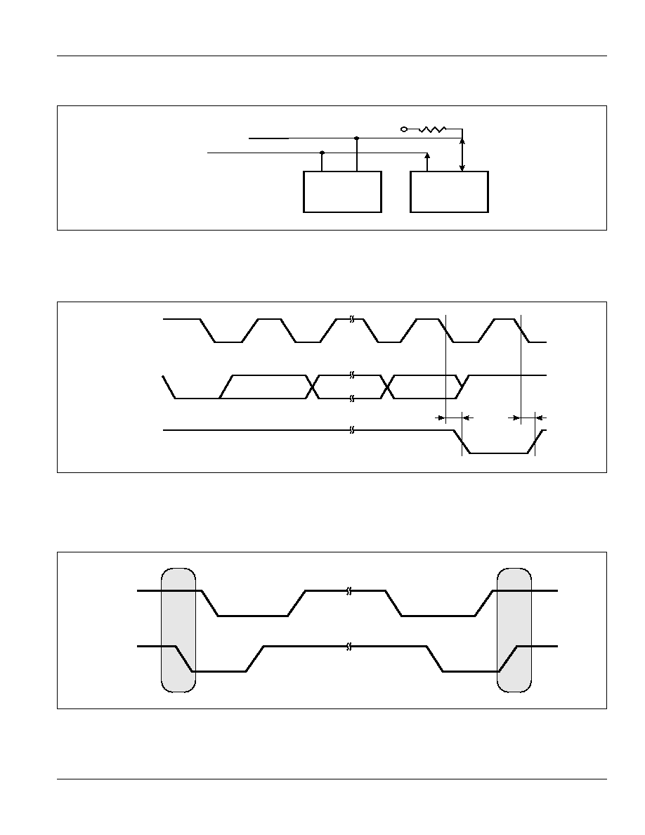
SCL
SDA
Master
Transmitter/
Receiver
IS24Cxx
Vcc
Figure 1. Typical System Bus Configuration
t
AA
Data Output
from
Transmitter
SCL from
Master
Data Output
from
Receiver
1
8
9
ACK
t
AA
Figure 2. Output Acknowledge
STOP
Condition
SCL
SDA
START
Condition
Figure 3. START and STOP Conditions