
Integrated Silicon Solution, Inc. -- 1-800-379-4774
1
PRELIMINARY INFORMATION
Rev. 00C
06/25/02
IS25C32-2/3
IS25C64-2/3
ISSI
Æ
Copyright © 2002 Integrated Silicon Solution, Inc. All rights reserved. ISSI reserves the right to make changes to this specification and its products at any time
without notice. ISSI assumes no liability arising out of the application or use of any information, products or services described herein. Customers are advised to
obtain the latest version of this device specification before relying on any published information and before placing orders for products.
32,768/65,536-BIT SPI SERIAL
ELECTRICALLY ERASABLE PROM
FEATURES
∑ 2.1 MHz Clock Rate
∑ Low power CMOS
-- Active current less than 3.0 mA (5.5V)
-- Standby current less than 10 µA (5.5V)
∑ Low-voltage Operation
-- IS25C64-3 & IS25C32-3 (Vcc = 2.5V to 5.5V)
-- IS25C64-2 & IS25C32-2 (Vcc = 1.8V to 5.5V)
∑ Block Write Protection
-- Protect 1/4, 1/2, or Entire Array
∑ 32 byte page write mode
∑ Serial Peripheral Interface (SPI) Compatible
-- Supports SPI Modes 0 (0,0) and 3 (1,1)
∑ Self timed write cycles (5 ms Typical)
∑ High-reliability
-- Endurance: 1 million cycles per byte
-- Data retention: 100 years
-- ESD protection >4000V
∑ Industrial temperature available
∑ 8-pin PDIP or SOIC, and 14-pin TSSOP Packages
PRELIMINARY INFORMATION
NOVEMBER 2001
The IS25C64-2 is a 1.8V (1.8V-5.5V) 64K-bit (8192x8)
electrically Erasable PROM, IS25C64-3 is a 2.5V (2.5V-
5.5V) 64K bit (8192x8) Electrically Erasable PROM,
IS25C32-2 is a 1.8V (1.8V-5.5V) 32K-bit (4096x8) Electri-
cally Erasable PROM, IS25C32-3 is a 2.5V (2.5V-5.5V)
32K-bit (4096x8) Electrically Erasable PROM.
The IS25Cxx (IS25C64-2, IS25C64-3, IS25C32-2 and
IS25C32-3) family is a low-cost and low voltage/low power
SPI Serial EEPROM. It is fabricated using ISSI's ad-
vanced CMOS EEPROM technology and provides a low
power and low voltage operation for low power industrial
and commercial application. The IS25Cxx family is
available in 8 pin PDIP, 8 Pin SOIC, and 14 pin TSSOP
packages.
The IS25Cxx is enabled through the Chip Select pin (
CS
)
and accessed via a 3-wire interface consisting of Serial
Data Input (SI), Serial Data Output (SO), and Serial Clock
(SCK). All programming cycles are completely self-timed,
and no separate ERASE cycle is required before WRITE.
BLOCK WRITE protection is enabled by programming the
status register with one of four configurations of write
protection. Separate program enable and program disable
instructions are provided for additional data protection.
Hardware data protection is provided via the
WP
pin to
protect against inadvertent write attempts to the status
register. The
HOLD
pin can suspend communications
without re-initializing the serial sequence.
DESCRIPTION
PRODUCT OFFERING OVERVIEW
Part No
Voltage
Speed
Standby ICC
Read ICC
Write ICC
Temperature
IS25C64-2
1.8V-5.5V
500 KHz
< 5 µA
1 mA
3 mA
C,I
IS25C64-3
2.5V-5.5V
2.1MHz
< 10 µA
1 mA
3 mA
C,I
IS25C32-2
1.8V-5.5V
500 KHz
< 5 µA
1 mA
3 mA
C,I
IS25C32-3
2.5V-5.5V
2.1MHz
< 10 µA
1 mA
3 mA
C,I
2
Integrated Silicon Solution, Inc. -- 1-800-379-4774
PRELIMINARY INFORMATION
Rev. 00C
06/25/02
IS25C32-2/3
IS25C64-2/3
ISSI
Æ
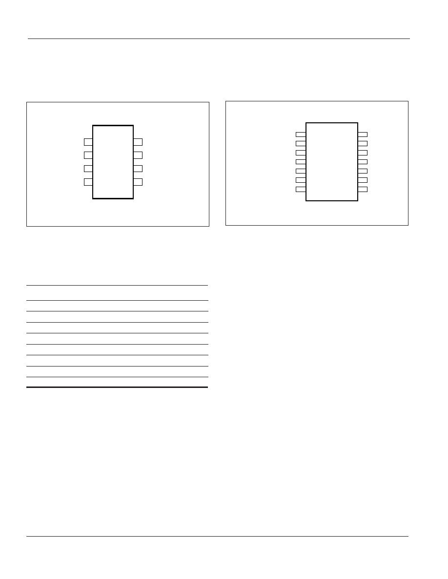
PIN CONFIGURATION
8-Pin DIP and SOIC
14-pin TSSOP
PIN DESCRIPTIONS
CS
Chip Select
SCK
Serial Data Clock
SI
Serial Data Input
SO
Serial Data Output
GND
Ground
V
CC
Power
WP
Write Protect
HOLD
Suspends Serial Input
NC
No Connect
PIN DESCRIPTIONS
Serial Clock (SCK) - This pin is used to synchronize the
communication between the microcontroller and the
IS25C64, IS25C32. Op-codes, byte addresses, or data
present on the SI pin and latched on the rising edge of the
SCK. Data on the SO pin is updated on the falling edge of
the SCK for SPI modes (0,0 & 1,1).
Serial Data Input (SI) - The SI pin is used to input all op-
codes, byte addresses, and data to be written to the
device. Input data is latched on the rising edge of the
serial clock for SPI modes (0,0 & 1,1).
Serial Data Output (SO) - The SO pin is used to transfer
data out of the device. During a read cycle, data is shifted
out on the falling edge of the serial clock for SPI modes (0,0
& 1,1).
Chip Select (
CS
): When the
CS
pin is low, the device is
enabled. When the
CS
pin is high the device is disabled.
CS
high takes the SO output pin to high impedance and
forces the devices into a Standby Mode (unless an
internal write operation is underway). The devices draws
zero current in the Standby mode. A high-to-low transition
on
CS
is required prior to any sequence being initiated. A
low-to-high transition on
CS
after a valid write sequence is
what initiates an internal write cycle.
1
2
3
4
8
7
6
5
CS
SO
WP
GND
VCC
HOLD
SCK
SI
14
13
12
11
10
9
8
1
2
3
4
5
6
7
CS
SO
NC
NC
NC
WP
GND
VCC
HOLD
NC
NC
NC
SCK
SI
Integrated Silicon Solution, Inc. -- 1-800-379-4774
3
PRELIMINARY INFORMATION
Rev. 00C
06/25/02
IS25C32-2/3
IS25C64-2/3
ISSI
Æ
PIN DESCRIPTIONS Continued:
Write Protect (
WP
) - The
WP
Pin will allow normal read/
write operations when held high. When
WP
is tied low and
the WPEN bit in the status register is set to "1", all write
operations to the status register are inhibited.
WP
going
low while CS is still low will interrupt a write to the status
register. If the internal write cycle has already been
initiated,
WP
going low will have no effect on any write
operation to the status register. The
WP
pin function is
blocked when the WPEN bit is set to 0. Figure 10
illustrates the
WP
timing sequence during a write opera-
tion.
Hold (
HOLD
): The
HOLD
pin is used to pause transmis-
sion to the device while in the middle of a serial sequence
without having to retransmit entire sequence at a later
time. To pause,
HOLD
must be brought low while SCK is
low. The SO pin is in a high impedance state during the
time the part is paused, and transition on the SI pins will
be ignored. To resume communication,
HOLD
is brought
high, while SCK is low. (
HOLD
should be held high any
time this function is not being used.)
HOLD
may be tied
high directly to Vcc or tied to Vcc through a resistor. The
HOLD
Timing Diagram illustrates hold timing sequence.
SERIAL INTERFACE DESCRIPTION
MASTER: This device that generates the serial clock.
SLAVE: Because the Serial Clock pin (SCK) is always an
input, the device always operates as a slave.
MSB: The Most Significant Bit (MSB) is the first bit
transmitted and received.
SERIAL OP-CODE: After the device is selected with CS
going low, the first byte will be received. This byte contains
the op-code that defines the operations to be performed.
INVALID OP-CODE: If an invalid op-code is received, no
data will be shifted into the device, and the serial output pin
(SO) will remain in a high impedance state until the falling
edge of CS is detected again. This will reinitialize the serial
communications.
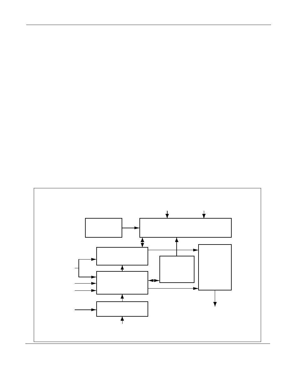
BLOCK DIAGRAM
STATUS
REGISTER
8192 x 8/4096 x 8
MEMORY ARRAY
HOLD
CS
WP
CLOCK
so
OUTPUT
BUFFER
SCK
SI
DATA
REGISTER
MODE
DECODE
LOGIC
GND
VCC
ADDRESS
DECODER

4
Integrated Silicon Solution, Inc. -- 1-800-379-4774
PRELIMINARY INFORMATION
Rev. 00C
06/25/02
IS25C32-2/3
IS25C64-2/3
ISSI
Æ
FUNCTIONAL DESCRIPTIONS
The IS25C32/64 utilizes an 8-bit instruction register. The
list of instructions and their operation codes are contained
in Table 1. All instructions, addresses, and data are
transferred with the MSB first and start with a high-to low
CS transition.
WRITE ENABLE (WREN):
This device will power-up in
the write disable state when VCC is applied. All program-
ming instructions must therefore be preceded by a Write
Enable instruction.
WRITE DISABLE (WRDI): To protect the device against
inadvertent writes, the Write Disable instruction disables
all programming modes. The WRDI instruction is indepen-
dent of the status of the
WP
pin.
READ STATUS REGISTER (RDSR):
The Read Status Register instruction provides access to
the status register. The READY/BUSY and Write Enable
status of the device can be determined by the RDSR
instruction. Similarly, the Block Write Protection bits
indicate the extent of protection employed. These bits are
set by using the WRSR instruction.
Table 1. Instruction Set
Instruction
Name
Format
Operation
WREN
0000 X110
Set Write Enable Latch
WRDI
0000 X100
Reset Write Enable Latch
RDSR
0000 X101
Read Status Register
WRSR
0000 X001
Write Status Register
READ
0000 X011 Read Data from Memory Array
WRITE
0000 X010
Write Data to Memory Array
Table 2. Status Register Format
Bit 7
Bit 6 Bit 5 Bit 4
Bit 3 Bit 2 Bit1 Bit 0
WPEN
x
x
x
BP1
BP0 WEN
RDY
Table 3. Read Status Register Bit Definition
Bit
Definition
Bit 0 (
RDY
)
Bit 0 = 0 (
RDY
) indicates the device is
READY. Bit 0 = 1 indicates the write
cycle is in progress.
Bit 1(WEN)
Bit 1 = 0 indicates the device is not
WRITE ENABLED. Bit 1 = 1 indicates
the device is WRITE ENABLED.
Bit 2 (BPO)
See Table 4
Bit 3 (BP1)
See Table 4
Bits 4 - 6 are 0s when the device is not an internal write cycle.
Bits 7 (WPEN) See Table 5.
Bits 0-7 are 1s during an internal write cycle.
Table 4. Status Register Format
Status
Register
Bits
Array Addresses Protected
Level
BP1
BP0
IS25C32
IS25C64
0
0
0
None
None
1(1/4)
0
1
0C00
1800
-0FFF
-1FFF
2(1/2)
1
0
0800
1000
-0FFF
-1FFF
3(All)
1
1
0000
0000
-0FFF
-1FFF
WRITE STATUS REGISTER (WRSR):
The WRSR in-
struction allows the user to select one of four levels of
protection. The device is divided into four array seg-
ments. One quarter (1/4), one half (1/2) or all of the
memory segments can be protected. Any of the data
within any selected segment will therefore be READ only.
The block write protection levels and corresponding
status register control bits are shown in Table 4.
The three bits, BP, BP1 and WPEN are nonvolatile
cells that have the same properties and functions as
the regular memory cells (e.g. WREN, twc, RDSR).

Integrated Silicon Solution, Inc. -- 1-800-379-4774
5
PRELIMINARY INFORMATION
Rev. 00C
06/25/02
IS25C32-2/3
IS25C64-2/3
ISSI
Æ
The WRSR instruction also allows the user to enable or
disable the write protect (
WP
) pin through the use of the
Write Protect Enable (WPEN) bit. Hardware write protec-
tion is enabled when the
WP
pin is low and the WPEN bit
is '"1". Hardware write protection is disabled when either
the
WP
pin is high or the WPEN bit is "0". When the device
is hardware write protected, writes to the Status Register,
including the Block Protect bits and the WPEN bit, and the
block-protected sections in the memory array are dis-
abled. Writes are only allowed to sections of the memory
which are not block-protected.
Note: When the WPEN bit is hardware write protected,
it cannot be changed back to "0", as long as the
WP
pin
is held low.
READ SEQUENCE (READ):
Reading the device via
the SO (Serial Output) pin requires the following
sequence. After the
CS
line is pulled low to select a
device, the READ op-code is transmitted via the SI line
followed by the byte address to be read (A15-A0, Refer
to Table 6). Upon completion, any data on the SI line
will be ignored. The data (D7-D0) at the specified
address is then shifted out onto the SO line. If only
one byte is to be read, the
CS
line should be driven
high after the data comes out. The READ sequence
can be continued since the byte address is automati-
cally incremented and data will continue to be shifted
out. When the highest address is reached, the address
counter will roll over to the lowest address allowing the
entire memory to be read in one continuous READ
cycle.
WRITE SEQUENCE (READ):
In order to program the
device, two sperate instructions must be executed.
First, the device must be write enabled via the Write
Enable (WREN) Instruction. Then a Write (WRITE)
Instruction may be executed. Also the address of the
memory location(s) to be programmed must be outside
the protected address field location selected by the
Block Write Protection Level. During an internal write
cycle, all commands will be ignored except the RDSR
instruction.
A Write Instruction requires the following sequence.
After the
CS
line is pulled low to select the device, the
WRITE op-code is transmitted via the SI line followed
by the byte address (A15-A0) and the data (D7-D0) to
be programmed (Refer to Table 6). Programming will
start after the
CS
pin is brought high. (The Low to High
transition of the
CS
pin must occur during the SCK low-
time immediately after clocking in the D0 (LSB) data bit.
The READY/BUSY status of the device can be deter-
mined by initiating a READ STATUS REGISTER
(RDSR) Instruction. If Bit 0 = 1, the WRITE cycle is still
in progress. If Bit 0 = 0 , the WRITE cycle has ended.
Only the READ STATUS REGISTER instruction is
enabled during the WRITE programming cycle.
The device is capable of the 32-byte PAGE WRITE
operation. After each byte of data is received, the five
low order address bits are internally incremented by
one; the high order bits of the address will remain
constant. If more than 32 bytes of data are transmit-
ted, the address counter will roll over the previously
written data will be overwritten. The device is auto-
matically returned to the write disable state at the
completion of a WRITE cycle.
NOTE: If the device is not Write enabled (WREN), the
device will ignore the Write instruction and will return to
the standby state, when
CS
is brought high. A new
CS
falling edge is required to re-initiate the serial communi-
cation.
Table 5. WPEN Operation
Protected
Unprotected Protected
WPEN
WP
WEN
Blocks
Blocks
Register
0
X
0
Protected
Protected
Protected
0
X
1
Protected
Writable
Writable
1
Low
0
Protected
Protected
Protected
1
Low
1
Protected
Writable
Protected
X
High
0
Protected
Protected
Protected
X
High
1
Protected
Writable
Writable
Table 6. Address Key
Name
IS25C32
IS25C64
A
N
A
11-
A
0
A
12-
A
0
Don't
A
15-
A
12
A
15-
A
13
Care Bits

6
Integrated Silicon Solution, Inc. -- 1-800-379-4774
PRELIMINARY INFORMATION
Rev. 00C
06/25/02
IS25C32-2/3
IS25C64-2/3
ISSI
Æ
ABSOLUTE MAXIMUM RATINGS
(1)
Symbol
Parameter
Value
Unit
V
S
Supply Voltage
-0.5 to +6.25
V
V
P
Voltage on Any Pin
≠1.0V to + 7.0V
V
T
BIAS
Temperature Under Bias
≠40 to +85
∞C
T
STG
Storage Temperature
≠65 to +150
∞C
I
OUT
Output Current
5
mA
Notes:
1. Stress greater than those listed under ABSOLUTE MAXIMUM RATINGS may cause perma-
nent damage to the device. This is a stress rating only and functional operation of the device at
these or any other conditions outside those indicated in the operational sections of this
specification is not implied. Exposure to absolute maximum rating conditions for extended
periods may affect reliability.
OPERATING RANGE (IS25C64-2 and IS25C32-2)
Range
Ambient Temperature
V
CC
Commercial
0∞C to +70∞C
1.8V to 5.5V
Industrial
≠40∞C to +85∞C
1.8V to 5.5V
CAPACITANCE
(1,2)
Symbol
Parameter
Conditions
Max.
Unit
C
IN
Input Capacitance
V
IN
= 0V
6
pF
C
OUT
Output Capacitance
V
OUT
= 0V
8
pF
Notes:
1. Tested initially and after any design or process changes that may affect these parameters and not 100%
tested.
2. Test conditions: T
A
= 25∞C, f = 1 MHz, Vcc = 5.0V.
OPERATING RANGE (IS25C64-3 and IS25C32-3)
Range
Ambient Temperature
V
CC
Commercial
0∞C to +70∞C
2.5V to 5.5V
Industrial
≠40∞C to +85∞C
2.5V to 5.5V

Integrated Silicon Solution, Inc. -- 1-800-379-4774
7
PRELIMINARY INFORMATION
Rev. 00C
06/25/02
IS25C32-2/3
IS25C64-2/3
ISSI
Æ
DC ELECTRICAL CHARACTERISTICS
Symbol Parameter
Test Conditions
Min.
Max.
Unit
V
OL
1
Output LOW Voltage
V
CC
= 1.8V, I
OL
= 0.15 mA
--
0.2
V
V
OL
2
Output LOW Voltage
V
CC
= 2.5V, I
OL
= 1.0 mA
--
0.4
V
V
O
H1
Output HIGH Voltage
V
CC
= 1.8V, I
O
H
= -100uA
V
CC
- 0.2
--
V
V
O
H2
Output HIGH Voltage
V
CC
= 2.5V, I
O
H
= -1mA
V
CC
- 0.8
--
V
V
IH
Input HIGH Voltage
V
CC
X
0.7 V
CC
+ 0.5
V
V
IL
Input LOW Voltage
≠1.0
V
CC
X
0.3
V
I
LI
Input Leakage Current
V
IN
= V
CC
max.
-3.0
3
µA
I
LO
Output Leakage Current
-3.0
3
µA
POWER SUPPLY CHARACTERISTICS
Symbol Parameter
Test Conditions
Min.
Max.
Unit
I
CC
1
Vcc Operating Current
READ at 500 KHz (Vcc=5V)
--
1.0
mA
I
CC
2
Vcc Operating Current
WRITE at 500 KHz (Vcc=5V)
--
3.0
mA
I
SB
1
Standby Current
Vcc = 1.8V
--
5
µA
I
SB
2
Standby Current
Vcc = 5.5V, V
IN
= V
CC
or GND
--
10
µA

8
Integrated Silicon Solution, Inc. -- 1-800-379-4774
PRELIMINARY INFORMATION
Rev. 00C
06/25/02
IS25C32-2/3
IS25C64-2/3
ISSI
Æ
AC Characteristics
Applicable over recommended operating range from T
A
= -40
∞
C to +85
∞
C, V
CC
= As Specified,
CL = 1 TTL Gate and 100 pF (unless otherwise noted).
1.8V
2.5V
Symbol
Parameter
Min
Max
Min
Max
Units
f
SCK
SCK Clock Frequency
0
0.5
0
2.1
MHz
t
RI
Input Rise Time
--
2
--
2
µs
t
FI
Input Fall Time
--
2
--
2
µs
t
WH
SCK High Time
800
--
200
--
ns
t
WL
SCK Low Time
800
--
200
--
ns
t
CS
CS
High Time
1000
--
250
--
ns
t
CSS
CS
Setup Time
1000
--
250
--
ns
t
CSH
CS
Hold Time
1000
--
250
--
ns
t
SU
Data In Setup Time
100
--
50
--
ns
t
H
Data In Hold Time
100
--
50
--
ns
t
HD
Hold
Setup Time
400
--
100
--
ns
t
CD
Hold
Time
400
--
300
--
ns
t
V
Output Valid
0
800
0
200
ns
t
HO
Output Hold Time
0
--
0
--
ns
t
LZ
Hold
to Output Low Z
0
200
0
200
ns
t
HZ
Hold
to Output High Z
--
200
--
200
ns
t
DIS
Output Disable Time
--
1000
--
250
ns
t
WC
Write Cycle Time
--
20
--
10
ms
Endurance
(1)
5.0V, 25∞C, Page Mode
1M
--
1M
--
Write Cycles
Integrated Silicon Solution, Inc. -- 1-800-379-4774
9
PRELIMINARY INFORMATION
Rev. 00C
06/25/02
IS25C32-2/3
IS25C64-2/3
ISSI
Æ
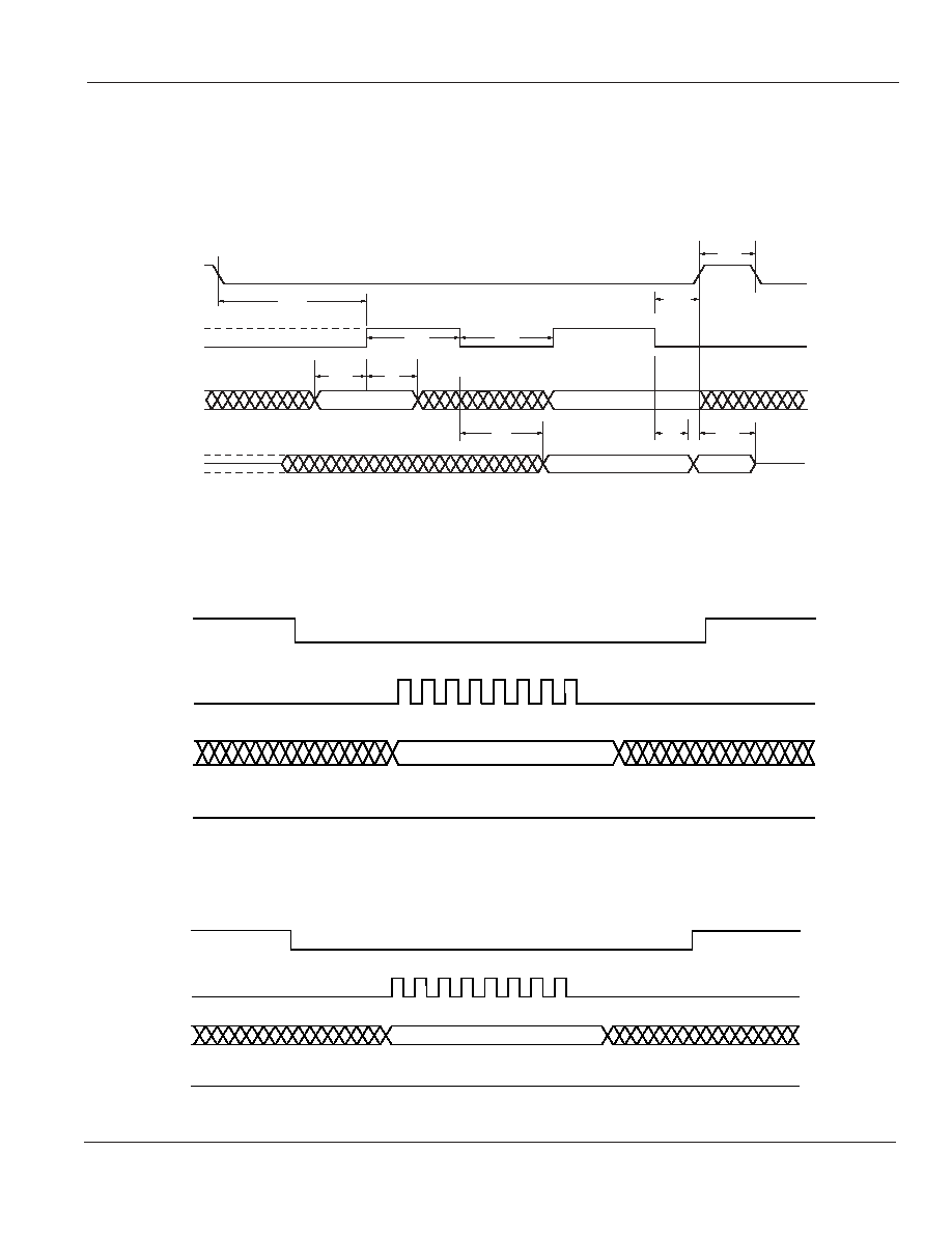
TIMING DIAGRAMS
WRDI Timing
WREN Timing
Synchronous Data Timing
CS
SK
D
IN
D
OUT
V
IH
V
IL
V
IH
V
IL
V
IH
V
IL
V
OH
V
OL
VALID IN
HIGH-Z
HIGH-Z
t
CSS
t
WH
t
WL
t
H
t
SU
t
CS
t
CSH
t
V
t
HO
t
DIS
HIGH-Z
WREN OP-CODE
CS
SK
D
IN
D
OUT
HIGH-Z
WRDI OP-CODE
CS
SK
D
IN
D
OUT
10
Integrated Silicon Solution, Inc. -- 1-800-379-4774
PRELIMINARY INFORMATION
Rev. 00C
06/25/02
IS25C32-2/3
IS25C64-2/3
ISSI
Æ
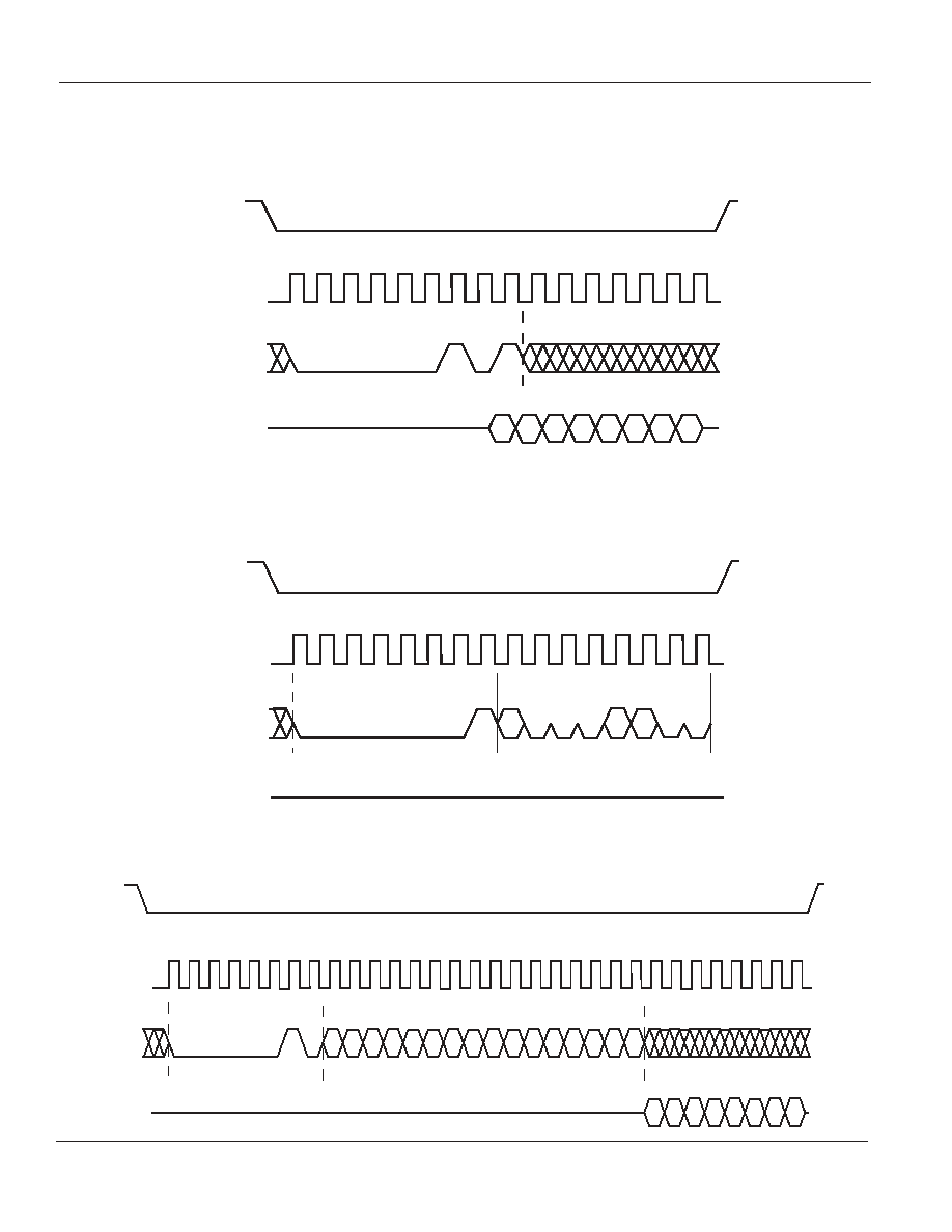
READ Timing
WRSR Timing
RDST Timing
CS
SK
Din
Dout
Instruction
7 6
5 4 3 2 1
0
DATA OUT
CS
SK
Din
Dout
Instruction
7 6
5 4 3 2 1 0
DATA IN
15 14 13 12 11 10 9 8 7 6 5 4 3 2 1 0
CS
SK
Din
Dout
Instruction
BYTE Address
7 6 5 4 3 2 1 0
DATA OUT

Integrated Silicon Solution, Inc. -- 1-800-379-4774
11
PRELIMINARY INFORMATION
Rev. 00C
06/25/02
IS25C32-2/3
IS25C64-2/3
ISSI
Æ
HOLD
Timing
WRITE Timing
7 6 5 4 3 2 1 0
15 14 13 12 11 10 9 8 7 6 5 4 3 2 1 0
CS
SK
Din
Dout
Instruction
BYTE Address
DATA IN
CS
SCK
HOLD
D
OUT
t
CD
t
HD
t
HZ
t
LZ
t
HD
t
CD

12
Integrated Silicon Solution, Inc. -- 1-800-379-4774
PRELIMINARY INFORMATION
Rev. 00C
06/25/02
IS25C32-2/3
IS25C64-2/3
ISSI
Æ
ORDERING INFORMATION
Commercial Range: 0∞C to +70∞C
Voltage
Frequency Range
Part Number
Package
500 KHz
1.8V
IS25C32-2P
300-mil Plastic DIP
to 5.5V
IS25C32-2G
Small Outline (JEDEC STD)
IS25C32-2Z
14-pin TSSOP
500 KHz
1.8V
IS25C64-2P
300-mil Plastic DIP
to 5.5V
IS25C64-2G
Small Outline (JEDEC STD)
IS25C64-2Z
14-pin TSSOP
2.1 MHz
2.5V
IS25C32-3P
300-mil Plastic DIP
to 5.5V
IS25C32-3G
Small Outline (JEDEC STD)
IS25C32-3Z
14-pin TSSOP
2.1 MHz
2.5V
IS25C64-3P
300-mil Plastic DIP
to 5.5V
IS25C64-3G
Small Outline (JEDEC STD)
IS25C64-3Z
14-pin TSSOP
ORDERING INFORMATION
Industrial Range: ≠40∞C to +85∞C
Voltage
Frequency Range
Part Number
Package
500 KHz
1.8V
IS25C32-2PI
300-mil Plastic DIP
to 5.5V
IS25C32-2GI
Small Outline (JEDEC STD)
IS25C32-2ZI
14-pin TSSOP
500 KHz
1.8V
IS25C64-2PI
300-mil Plastic DIP
to 5.5V
IS25C64-2GI
Small Outline (JEDEC STD)
IS25C64-2ZI
14-pin TSSOP
2.1 MHz
2.5V
IS25C32-3PI
300-mil Plastic DIP
to 5.5V
IS25C32-3GI
Small Outline (JEDEC STD)
IS25C32-3ZI
14-pin TSSOP
2.1 MHz
2.5V
IS25C64-3PI
300-mil Plastic DIP
to 5.5V
IS25C64-3GI
Small Outline (JEDEC STD)
IS25C64-3ZI
14-pin TSSOP
ISSI
Æ
Integrated Silicon Solution, Inc.
2231 Lawson Lane
Santa Clara, CA 95054
Tel: 1-800-379-4774
Fax: (408) 588-0806
E-mail: sales@issi.com
www.issi.com