
Integrated Silicon Solution, Inc. -- 1-800-379-4774
1
Preliminary Information
Rev. 00E
02/07/06
IS25C32A
IS25C64A
ISSI
Æ
Copyright © 2006 Integrated Silicon Solution, Inc. All rights reserved. ISSI reserves the right to make changes to this specification and its products at any time
without notice. ISSI assumes no liability arising out of the application or use of any information, products or services described herein. Customers are advised to
obtain the latest version of this device specification before relying on any published information and before placing orders for products.
32K-BIT/64K-BIT SPI SERIAL
ELECTRICALLY ERASABLE PROM
FEATURES
∑ Serial Peripheral Interface (SPI) Compatible
-- Supports SPI Modes 0 (0,0) and 3 (1,1)
∑ Wide-voltage Operation
-- Vcc = 1.8V to 5.5V
∑ Low power CMOS
-- Active current less than 3.0 mA (2.5V)
-- Standby current less than 2.0 µA (2.5V)
∑ Block Write Protection
-- Protect 1/4, 1/2, or Entire Array
∑ 32 byte page write mode
-- Partial page writes allowed
∑ 10 MHz Clock Rate (5V)
∑ Self timed write cycles (5 ms Typical)
∑ High-reliability
-- Endurance: 1 million cycles per byte
-- Data retention: 100 years
∑ Industrial and Automotive temperature ranges
∑ 8-pin PDIP, 8-pin SOIC, and 8-pin TSSOP Packages
available
∑ Lead-free available
Preliminary Information
March 2006
The IS25C32A and IS25C64A are electrically erasable
PROM devices that use the Serial Peripheral Interface
(SPI) for communications. The IS25C32A is 32Kbit
(4096 x 8) and the IS25C64A is 64Kbit (8192 x 8). The
IS25C32A/64A EEPROMs are offered in a wide
operating voltage range of 1.8V to 5.5V to be compatible
with most application voltages. ISSI designed the
IS25C32A/64A to be an efficient SPI EEPROM solution.
The devices are packaged in 8-pin PDIP, 8-pin SOIC,
and 8-pin TSSOP.
The functional features of the IS25C32A/64A allow them
to be among the most advanced serial non-volatile
memories available. Each device has a Chip-Select
(
CS) pin, and a 3-wire interface of Serial Data In (SI),
Serial Data Out (SO), and Serial Clock (SCK). While
the 3-wire interface of the IS25C32A/64A provides for
high-speed access, a
HOLD pin allows the memories to
ignore the interface in a suspended state; later the
HOLD pin re-activates communication without re-
initializing the serial sequence. A Status Register
facilitates a flexible write protection mechanism, and a
device-ready bit (
RDY).
DESCRIPTION
2
Integrated Silicon Solution, Inc. -- 1-800-379-4774
Preliminary Information
Rev. 00E
02/07/06
IS25C32A
IS25C64A
ISSI
Æ
Write Protect (
WP
WP
WP
WP
WP): The purpose of this input signal is
to initiate Hardware Write Protection mode. This mode
prevents the Block Protection bits and the WPEN bit in
the Status Register from being altered. To cause
Hardware Write Protection,
WP must be Low at the same
time WPEN is 1.
WP may be hardwired to Vcc or GND.
HOLD (
HOLD
HOLD
HOLD
HOLD
HOLD): This input signal is used to suspend the
device in the middle of a serial sequence and temporarily
ignore further communication on the bus (SI, SO, SCK).
Together with Chip Select, the
HOLD signal allows
multiple slaves to share the bus.
The
HOLD signal
transitions must occur only when SCK is Low, and be
held stable during SCK transitions. (See Figure 8 for
Hold timing) To disable this feature,
HOLD may be
hardwired to Vcc.
PIN DESCRIPTIONS
CS
Chip Select
SCK
Serial Data Clock
SI
Serial Data Input
SO
Serial Data Output
GND
Ground
V
CC
Power
WP
Write Protect
HOLD
Suspends Serial Input
PIN DESCRIPTIONS
Serial Clock (SCK): This timing signal provides syn-
chronization between the microcontroller and IS25C32A/
64A. Op-Codes, byte addresses, and data are latched
on SI with a rising edge of the SCK. Data on SO is
refreshed on the falling edge of SCK for SPI modes (0,0)
and (1,1).
Serial Data Input (SI): This is the input pin for all data
that the IS25C32A/64A is required to receive.
Serial Data Output (SO): This is the output pin for all
data transmitted from the IS25C32A/64A.
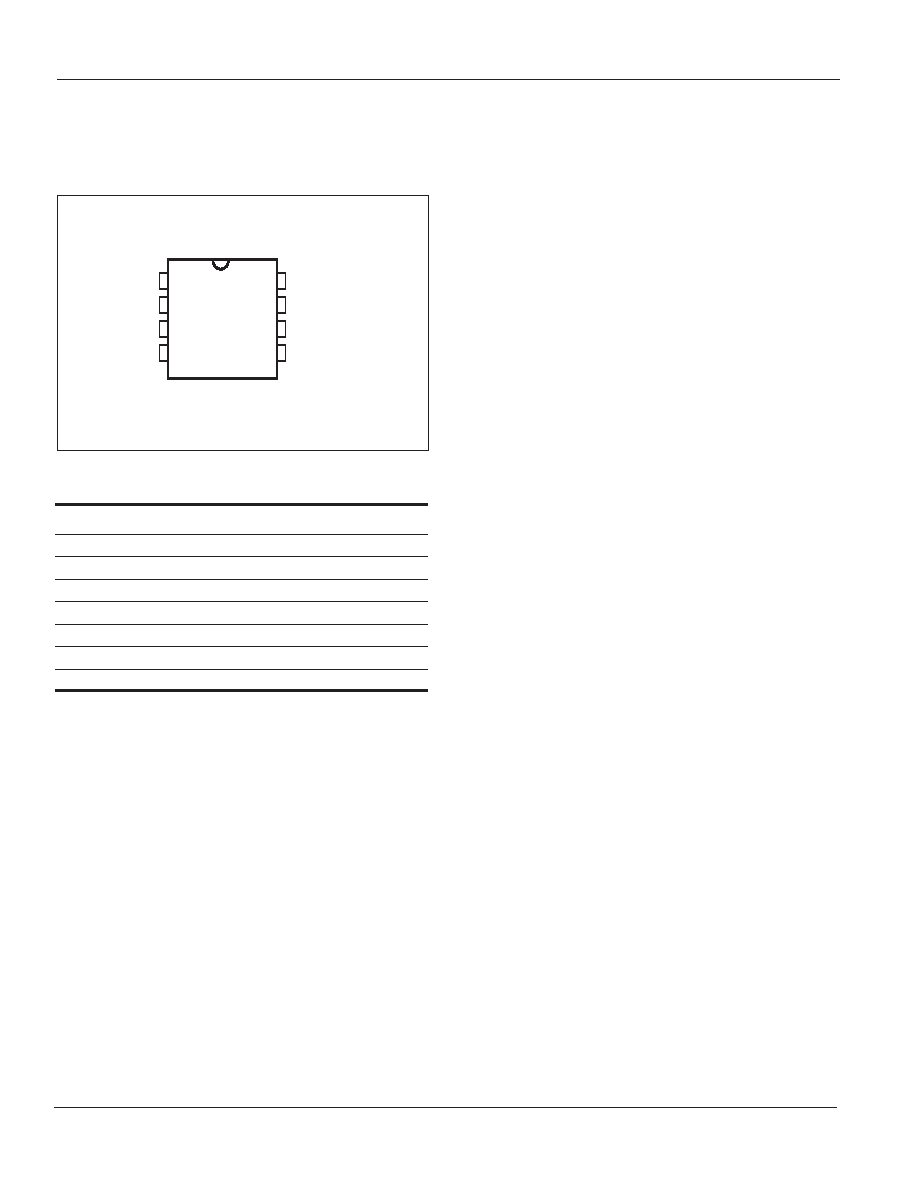
PIN CONFIGURATION
8-Pin DIP, SOIC, and TSSOP
Chip Select (
CS
CS
CS
CS
CS): The CS pin activates the device.
Upon power-up,
CS should follow Vcc. When the device
is to be enabled for instruction input, the signal requires
a High-to-Low transition. While
CS is stable Low, the
master and slave will communicate via SCK, SI, and SO
signals. Upon completion of communication,
CS must
be driven High. At this moment, the slave device may
start its internal write cycle. When
CS is high, the
device enters a power-saving standby mode, unless an
internal write operation is underway. During this mode,
the SO pin becomes high impedance.
1
2
3
4
8
7
6
5
CS
SO
WP
GND
VCC
HOLD
SCK
SI
Integrated Silicon Solution, Inc. -- 1-800-379-4774
3
Preliminary Information
Rev. 00E
02/07/06
IS25C32A
IS25C64A
ISSI
Æ
SERIAL INTERFACE DESCRIPTION
MASTER: The device that provides a clock signal.
SLAVE: The IS25C32A/64A is a slave because the
clock signal is an input.
TRANSMITTER/RECEIVER: The IS25C32A/64A has
both data input (SI) and data output (SO).
MSB: The most significant bit. It is always the first bit
transmitted or received.
OP-CODE: The first byte transmitted to the slave
following CS transition to LOW. If the OP-CODE is a
valid member of the IS25C32A/64A instruction set (Table
3), then it is decoded appropriately. If the OP-CODE is
not valid, and the SO pin remains in high impedance.
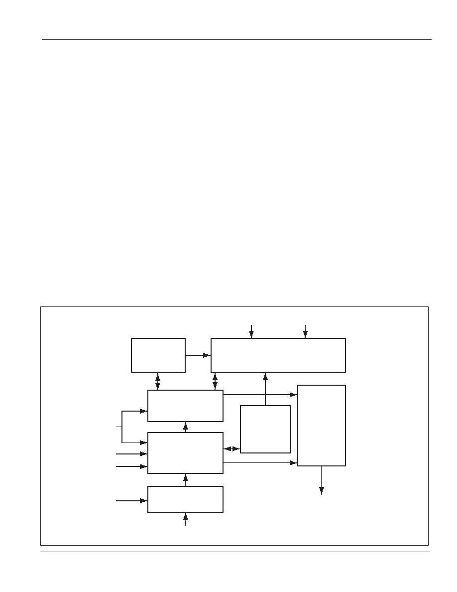
BLOCK DIAGRAM
STATUS
REGISTER
8192 x 8/4096 x 8
MEMORY ARRAY
HOLD
CS
WP
CLOCK
SO
OUTPUT
BUFFER
SCK
SI
DATA
REGISTER
MODE
DECODE
LOGIC
GND
VCC
ADDRESS
DECODER

4
Integrated Silicon Solution, Inc. -- 1-800-379-4774
Preliminary Information
Rev. 00E
02/07/06
IS25C32A
IS25C64A
ISSI
Æ
STATUS REGISTER
Table 1. Status Register Format
Bit 7
Bit 6 Bit 5 Bit 4
Bit 3 Bit 2
Bit1 Bit 0
WPEN
X
X
X
BP1
BP0
WEN
RDY
The status register contains 8-bits for write protection
control and write status. (See Table 1). It is the only
region of memory other than the main array that is
accessible by the user.
The Status Register is Read-Only if either: a) Hardware
Write Protection is enabled or b) WEN is set to 0. If
neither is true, it can be modified by a valid instruction.
Ready (
RDY
RDY
RDY
RDY
RDY), Bit 0: When RDY = 1, it indicates that
the device is busy with a write cycle.
RDY = 0 indi-
cates that the device is ready for an instruction. If
RDY
= 1, the only command that will be handled by the
device is Read Status Register.
Don't Care, Bits 4-6: Each of these bits can receive
either 0 or 1, but values will not be retained. When
these bits are read from the register, they are always 0.
Write Protect Enable (WPEN), Bit 7: This bit can be
used in conjunction with
WP pin to enable Hardware
Write Protection, which causes the Status Register to
be read-only. The memory array is not protected by this
mode. Hardware Write Protection requires that
WP = 0
and WPEN = 1; it is disabled otherwise. Note: WPEN
cannot be changed from 1 to 0 if the
WP pin is already
set to Low. (See Table 4 for data protection relationship)
Notes:
1. X = Don't care bit.
2. During internal write cycles, bits 0 to 7 are temporarily 1's.
Block Protect (BP1, BP0), Bits 2-3: Together, these
bits represent one of four block protection configurations
implemented for the memory array. (See Table 2 for
details.)
BP0 and BP1 are non-volatile cells similar to regular
array cells, and factory programmed to 0. The block of
memory defined by these bits is always protected,
regardless of the setting of WPEN,
WP , or WEN.
Table 2. Block Protection
Status
Register
Bits
Array Addresses Protected
Level
BP1
BP0
IS25C32A
IS25C64A
0
0
0
None
None
1(1/4)
0
1
0C00h
1800h
-0FFFh
-1FFFh
2(1/2)
1
0
0800h
1000h
-0FFFh
-1FFFh
3(All)
1
1
0000h
0000h
-0FFFh
-1FFFh
Write Enable (WEN), Bit 1: This bit represents the
status of device write protection. If WEN = 0, the Status
Register and the entire array is protected from modifica-
tion, regardless of the setting of WPEN,
WP pin, or block
protection. The only way to set WEN to 1 is via the
Write Enable command (WREN). WEN is reset to 0
upon power-up.

Integrated Silicon Solution, Inc. -- 1-800-379-4774
5
Preliminary Information
Rev. 00E
02/07/06
IS25C32A
IS25C64A
ISSI
Æ
WRITE ENABLE (WREN)
When Vcc is initially applied, the device powers up with
both status register and entire array in a write-disabled
state. Upon completion of Write Disable (WRDI), Write
Status Register (WRSR), or Write Data to Array
(WRITE), the device resets the WEN bit in the Status
Register to 0. Prior to any data modification, a WREN
instruction is necessary to set WEN to 1. (See Figure 2
for timing).
WRITE DISABLE (WRDI)
The device can be completely protected from modifica-
tion by resetting WEN to 0 through the WRDI instruc-
tion. (See Figure 3 for timing).
READ STATUS REGISTER (RDSR)
The Read Status instruction tells the user the status of
Write Protect Enable, the Block Protection setting (see
Table 2), the Write Enable state, and the
RDY status.
RDSR is the only instruction accepted when a write
cycle is underway. It is recommended that the status of
Write Enable and
RDY be checked, especially prior to
an attempted modification of data. The 8 bits of the
Status Register can be repeatedly output on SO after
the initial Op-code. (See Figure 4 for timing).
Table 3. Instruction Set
Name
Op-code
Operation
Address
Data(SI)
Data (SO)
WREN
0000 X110
Set Write Enable Latch
-
-
-
WRDI
0000 X100
Reset Write Enable Latch
-
-
-
RDSR
0000 X101
Read Status Register
-
-
D7-D0,...
WRSR
0000 X001
Write Status Register
-
D7-D0
-
READ
0000 X011
Read Data from Array
A15-A0
-
D7-D0,...
WRITE
0000 X010
Write Data to Array
A15-A0
D7-D0,...
-
DEVICE OPERATION
T
he operations of the IS25C32A/64A are controlled by a set of instructions that are clocked-in serially SI pin. (See
Table 3). To begin an instruction, the chip select (
CS) should be dropped Low. Subsequently, each Low-to-High
transition of the clock (SK) will latch a stable value on the SI pin. After the 8-bit op-code, it may be appropriate to
continue to input an address or data to SI, or to output data from SO. During data output, values appear on the falling
edge of SK. All bits are transferred with MSB first. Upon the last bit of communication, but prior to any following Low-
to-High transition of SK,
CS should be raised High to end the transaction. The device then would enter Standby Mode
if no internal programming were underway.
1. X = Don't care bit. For consistency, it is best to use "0".
2. Some address bits are don't care. See Table 5.
3. If the bits clocked-in for an op-code are invalid, SO remains high impedance, and upon CS going High there is no
affect. A valid op-code with an invalid number of bits clocked-in for address or data will cause an attempt to modify the
array or Status Register to be ignored.