ISSI
Æ
IS27HC010
Integrated Silicon Solution, Inc.
1
EP009-1F
07/18/97
ISSI reserves the right to make changes to its products at any time without notice in order to improve design and supply the best possible product. We assume no responsibility for any errors which
may appear in this publication. © Copyright 1997, Integrated Silicon Solution, Inc.
FEATURES
∑ Fast read access time: 30 ns
∑ Pin compatible with the IS27C010
∑ High-speed write programming
-- Typically less than 30 seconds
∑ Industrial and commercial temperature ranges
available
∑
±
10% power supply tolerance
∑ JEDEC-approved pinout
∑ Standard 32-pin DIP, PLCC, and TSOP
packages
DESCRIPTION
The
ISSI
IS27HC010 is an ultra-high-speed 1 megabit (128K-
word by 8-bit) Ultraviolet Erasable CMOS Programmable
Read-Only Memory. It utilizes the standard JEDEC pinout
making it functionally compatible with the IS27C010, but with
significantly faster access capability. This superior random
access capability results from a focused high-speed design.
This offers users bipolar speeds with higher density, lower
cost, and proven reliability.
The device is ideal for use with the faster processors. Design-
ers may take full advantage of high-speed digital signal
processors and microprocessors by allowing code to be
executed at full speed directly out of EPROM. Typical applica-
tions include laser printers, switching networks, graphics,
workstations, high-speed modems, and digital signal process-
ing.
The IS27HC010 uses
ISSI
'
s write programming algorithm
which allows the entire chip to be programmed in typically less
than 30 seconds.
This product is available inOne-Time Programmable (OTP)
PDIP, PLCC, and TSOP packages over commercial and
industrial temperature ranges.
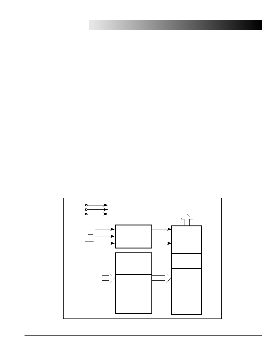
IS27HC010
131,072 x 8 HIGH-SPEED CMOS EPROM
ISSI
Æ
VCC
GND
VPP
OE
OUTPUT ENABLE
CHIP ENABLE
AND
PROG LOGIC
1,048,576-BIT
CELL MATRIX
CE
PGM
OUTPUT
BUFFERS
Y
GATING
X
DECODER
Y
DECODER
17
A0-A16
8
DQ0-DQ7
FUNCTIONAL BLOCK DIAGRAM
JULY 1997
ISSI
Æ
IS27HC010
2
Integrated Silicon Solution, Inc.
EP009-1F
07/18/97
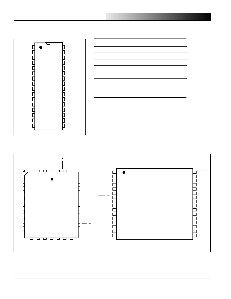
PIN CONFIGURATIONS
32-Pin DIP
1
2
3
4
5
6
7
8
9
10
11
12
13
14
15
16
32
31
30
29
28
27
26
25
24
23
22
21
20
19
18
17
VPP
A16
A15
A12
A7
A6
A5
A4
A3
A2
A1
A0
DQ0
DQ1
DQ2
GND
VCC
PGM (P)
NC
A14
A13
A8
A9
A11
OE (G)
A10
CE (E)
DQ7
DQ6
DQ5
DQ4
DQ3
PIN DESCRIPTIONS
A0-A16
Address Inputs
CE
(
E
)
Chip Enable Input
DQ0-DQ7
Data Inputs/Outputs
OE
(
G
)
Output Enable Input
PGM
(
P
)
Program Enable Input
Vcc
Power Supply Voltage
V
PP
Program Supply Voltage
GND
Ground
NC
No Internal Connection
32-Pin PLCC
DQ1
DQ2
GND
DQ3
DQ4
DQ5
DQ6
A12
A15
A16
VPP
VCC
PGM (P)
NC
A14
A13
A8
A9
A11
OE (G)
A10
CE (E)
DQ7
A7
A6
A5
A4
A3
A2
A1
A0
DQ0
5
6
7
8
9
10
11
12
13
29
28
27
26
25
24
23
22
21
INDEX
4
3
2
1
32
31
30
14
15
16
17
18
19
20
32-Pin TSOP
1
2
3
4
5
6
7
8
9
10
11
12
13
14
15
16
32
31
30
29
28
27
26
25
24
23
22
21
20
19
18
17
A11
A9
A8
A13
A14
NC
PGM (P)
VCC
VPP
A16
A15
A12
A7
A6
A5
A4
OE (G)
A10
CE (E)
DQ7
DQ6
DQ5
DQ4
DQ3
GND
DQ2
DQ1
DQ0
A0
A1
A2
A3

ISSI
Æ
IS27HC010
Integrated Silicon Solution, Inc.
3
EP009-1F
07/18/97
FUNCTIONAL DESCRIPTION
Erasing the IS27HC010
In order to clear all locations of their programmed contents,
it is necessary to expose the IS27HC010 to an ultraviolet
light source. A dosage of 30W - sec/cm
2
is required to
completely erase the IS27HC010. This dosage can be
obtained by exposure to an ultraviolet lamp-wavelength of
2537 Angstroms (≈)--with intensity of 12,000
µ
W/cm
2
for
30 to 40 minutes. The IS27HC010 should be directly under
and about one inch from the source and all filters should be
removed from the UV light source prior to erasure.
It is important to note that the IS27HC010, and similar
devices, will erase with light sources having wavelengths
shorter than 4000≈. The exposure to fluorescent light and
sunlight will eventually erase the IS27HC010 and expo-
sure to them should be prevented to realize maximum
system reliability. If used in such an environment, the
package window should be covered by an opaque label or
substance.
Programming the IS27HC010
Upon delivery, or after each erasure, the IS27HC010 has
1,048,576 bits in the "ONE", or HIGH state. "ZEROs" are
loaded into the IS27HC010 through the procedure of
programming.
The programming mode is entered when 12.75
±
0.25V is
applied to the V
PP
pin, V
CC
= 6.25V,
CE
and
PGM
is at V
IL
,
and
OE
is at V
IH
. For programming, the data to be pro-
grammed is applied eight bits in parallel to the data output
pins.
The write programming algorithm reduces programming
time by using 100
µ
s programming pulses followed by a
byte verification to determine whether the byte has been
successfully programmed. If the data does not verify, an
additional pulse is applied for a maximum of 25 pulses.
This process is repeated while sequencing through each
address of the EPROM.
The write programming algorithm programs and verifies at
V
CC
= 6.25V and V
PP
= 12.75V. After the final address is
completed, all byte are compared to the original data with
V
CC
= 5.25V.
Program Inhibit
Programming of multiple IS27HC010s in parallel with
different data is also easily accomplished. Except for
CE
,
all like inputs of the parallel IS27HC010 may be common.
A TTL low-level program pulse applied to an IS27HC010
CE
input with V
PP
= 12.75
±
0.25V,
PGM
LOW and
OE
HIGH will program that IS27HC010. A high-level
CE
input
inhibits the other IS27HC010 from being programmed.
Program Verify
A verify should be performed on the programmed bits to
determine that they were correctly programmed. The
verify should be performed with
OE
and
CE
at V
IL
,
PGM
at
V
IH
, and V
PP
between 12.5V and 13.0V.
Auto Select Mode
The auto select mode allows the reading out of a binary
code from an EPROM that will identify its manufacturer
and type. This mode is intended for use by programming
equipment for the purpose of automatically matching the
device to be programmed with its corresponding program-
ming algorithm. This mode is functional in the 25
∞
C
±
5
∞
C
ambient temperature range that is required when pro-
gramming the IS27HC010.
To activate this mode, the programming equipment must
force 12.0
±
0.5V on address line A9 of the IS27HC010.
Two identifier bytes may then be sequenced from the
device outputs by toggling address line A0 from V
IL
to V
IH
.
All other address lines must be held at V
IL
during auto
select mode.
Byte 0 (A0 = V
IL
) represents the manufacturer code, and
byte 1 (A0 = V
IH
), the device identifier code. For the
IS27HC010, these two identifier bytes are given in the
Mode Select table. All identifiers manufacturer and device
codes will possess odd parity, with the MSB (DQ7) defined
as the parity bit.
Read Mode
The IS27HC010 has two control functions, both of which
must be logically satisfied in order to obtain data at the
outputs. Chip Enable (
CE
) is the power control and should
be used for device selection. Assuming that addresses are
stable, address access time (t
ACC
) is equal to the delay
from
CE
to output (t
CE
). Output Enable (
OE
) is the output
control and should be used to get data to the output pins,
independent of device selection. Data is available at the
outputs t
OE
after the falling edge of
OE
assuming that
CE
has been LOW and addresses have been stable for at
least t
ACC
≠ t
OE
.
Standby Mode
The IS27HC010 has a standby mode which reduces the
maximum V
CC
active current. It is placed in standby mode
when
CE
is at V
IH
. The amount of current drawn in standby
mode depends on the frequency and the number of
address pins switching. The IS27HC010 is specified with
50% of the address lines toggling at 10 MHz. A reduction
of the frequency or quantity of address lines toggling will
significantly reduce the actual standby current.
ISSI
Æ
IS27HC010
4
Integrated Silicon Solution, Inc.
EP009-1F
07/18/97
Output OR-Tieing
To accommodate multiple memory connections, a two-
line control function is provided to allow for:
1.
Low memory power dissipation, and
2.
Assurance that output bus contention will not
occur.
It is recommended that
CE
be decoded and used as the
primary device-selecting function, while
OE
be made a
common connection to all devices in the array and con-
nected to the READ line from the system control bus. This
assures that all deselected memory devices are in their
low-power standby mode and that the output pins are only
active when data is desired from a particular memory
device.
System Applications
During the switch between active and standby conditions,
transient current peaks are produced on the rising and
falling edges of Chip Enable. The magnitude of these
transient current peaks is dependent on the output capaci-
tance loading of the device at a minimum, a 0.1
µ
F ceramic
capacitor (high-frequency, low inherent inductance) should
be used on each device between V
CC
and GND to mini-
mize transient effects. In addition, to overcome the voltage
drop caused by the inductive effects of the printed circuit
board traces on EPROM arrays, a 4.7
µ
F bulk electrolytic
capacitor should be used between V
CC
and GND for each
eight devices. The location of the capacitor should be
close to where the power supply is connected to the array.
TRUTH TABLE
(1,2)
Mode
CE
CE
CE
CE
CE
OE
OE
OE
OE
OE
PGM
PGM
PGM
PGM
PGM
A0
A9
V
PP
Outputs
Read
V
IL
V
IL
X
X
X
V
CC
D
OUT
Output Disable
V
IL
V
IH
X
X
X
V
CC
Hi-Z
Standby
V
IH
X
X
X
X
V
CC
Hi-Z
Program
V
IL
V
IH
V
IL
X
X
V
PP
D
IN
Program Verify
V
IL
V
IL
V
IH
X
X
V
PP
D
OUT
Program Inhibit
V
IH
X
X
X
X
V
PP
Hi-Z
Auto Select
(3,5)
Manufacturer Code
V
IL
V
IL
X
V
IL
V
H
V
CC
D5H
Device Code
V
IL
V
IL
X
V
IH
V
H
V
CC
0EH
Notes:
1. V
H
= 12.0V
±
0.5V.
2. X = Either V
IH
or V
IL
.
3. A1-A8 = A10-A16 = V
IL
.
4. See DC Programming Characteristics for V
PP
voltage during programming.
5. The IS27HC010 can use the same write algorithm during program as other IS27C010 or IS27010 devices.
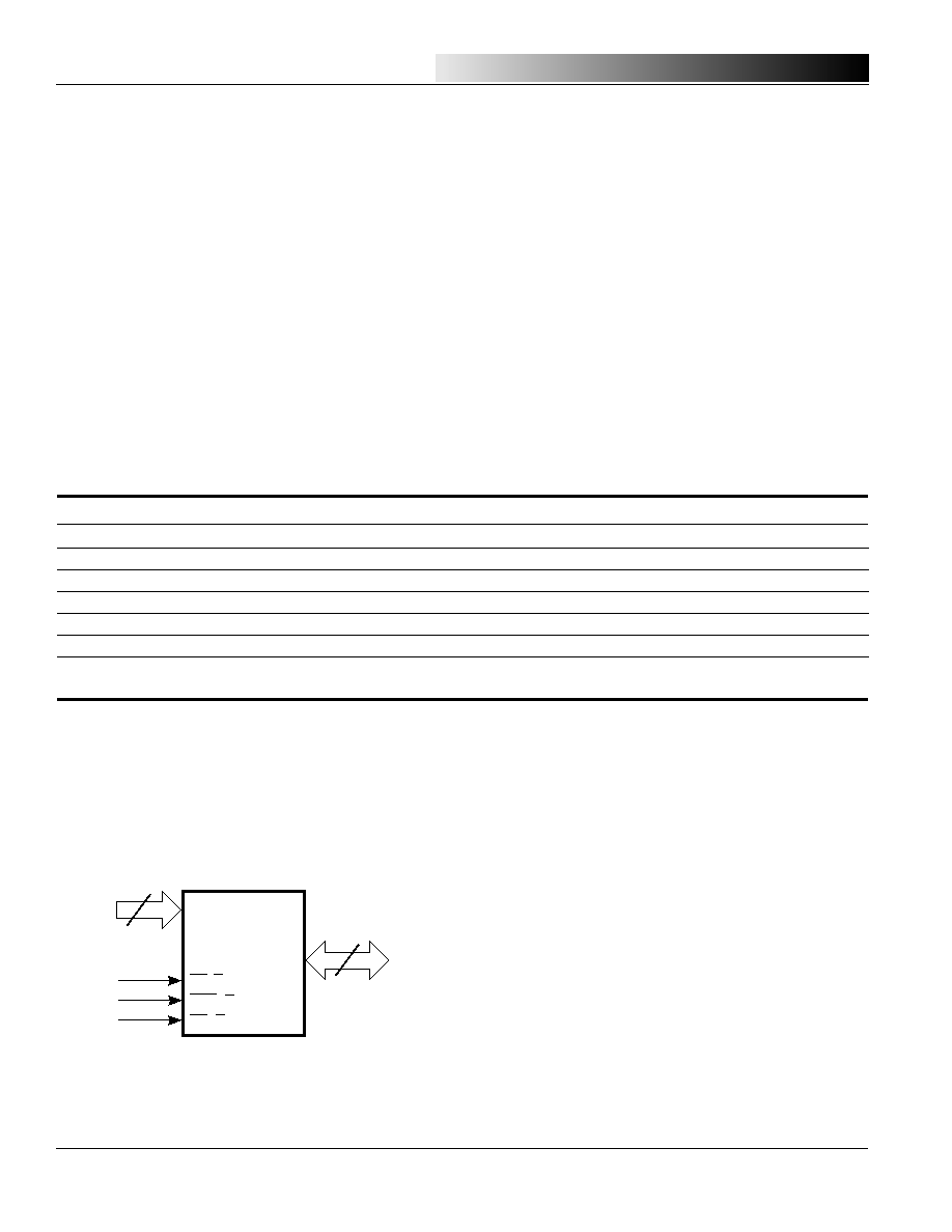
LOGIC SYMBOL
17
DQ0-DQ7
A0-A16
CE (E)
PGM (P)
OE (G)
8

ISSI
Æ
IS27HC010
Integrated Silicon Solution, Inc.
5
EP009-1F
07/18/97
ABSOLUTE MAXIMUM RATINGS
(1)
Symbol
Parameter
Value
Unit
V
TERM
Terminal Voltage with Respect to GND
All pins except A9 and V
PP
≠0.6 to V
CC
+ 0.5
(2)
V
V
PP
V
CC
≠ 0.3 to 13.5
(2,3)
V
A9
≠0.6 to 13.5
(2,3)
V
V
CC
≠0.6 to 7.0
(2)
V
T
A
Ambient Temperature with Power Applied
≠65 to +125
∞
C
T
STG
Storage Temperature (OTP)
≠65 to +125
∞
C
T
STG
Storage Temperature (All others)
≠65 to +150
∞
C
Notes:
1. Stress greater than those listed under ABSOLUTE MAXIMUM RATINGS may cause permanent damage to the
device. This is a stress rating only and functional operation of the device at these or any other conditions above
those indicated in the operational sections of this specification is not implied. Exposure to absolute maximum
rating conditions for extended periods may affect reliability.
2. Minimum DC input voltage is ≠0.5V. During transitions, inputs may undershoot to ≠2.0V for periods less than 10
ns. Maximum DC voltage on output pins is V
CC
+ 0.5V which may overshoot to V
CC
+ 2.0V for periods less than
10 ns.
3. Maximum DC voltage on A9 or V
PP
may overshoot to +13.5V for periods less than 10 ns.
OPERATING RANGE
Range
Ambient Temperature
V
CC
Commercial
0
∞
C to +70
∞
C
5V
±
10%
Industrial
(1)
≠40
∞
C to +85
∞
C
5V
±
10%
Note:
1. Operating ranges define those limits between which the
functionally of the device is guaranteed.
DC ELECTRICAL CHARACTERISTICS
(1,2,3)
(Over Operating Range)
Symbol Parameter
Test Conditions
Min.
Max.
Unit
V
OH
Output HIGH Voltage
V
CC
= Min., I
OH
= ≠4 mA
2.4
--
V
V
OL
Output LOW Voltage
V
CC
= Min., I
OL
= 12 mA
--
0.45
V
V
IH
Input HIGH Voltage
(4)
2.0
V
CC
+ 0.5
V
V
IL
Input LOW Voltage
(4)
≠0.3
0.8
V
I
LI
Input Load Current
V
IN
= 0V to +V
CC
--
5.0
µ
A
I
LO
Output Leakage Current
V
OUT
= 0V to +V
CC
--
10
µ
A
Notes:
1. V
CC
must be applied simultaneously or before V
PP
and removed simultaneously or after V
PP
. Never try to force V
PP
LOW to 1V
below V
CC
. Manufacturer suggests to tie V
PP
and Vcc together during the READ operation.
2. Caution: the IS27HC010 must not be removed from (or inserted into) a socket when V
CC
or V
PP
is applied.
3. Minimum DC input voltage is ≠0.5V. During transitions, the inputs may undershoot to ≠2.0V for periods less than 10 ns.
Maximum DC voltage on output pins is V
CC
+ 0.5V which may overshoot to V
CC
+ 2.0V for periods less than 10 ns.
4. Tested under static DC conditions.