Copyright © 2003 Integrated Silicon Solution, Inc. All rights reserved. ISSI reserves the right to make changes to this specification and its products at any time
without notice. ISSI assumes no liability arising out of the application or use of any information, products or services described herein. Customers are advised to
obtain the latest version of this device specification before relying on any published information and before placing orders for products.
Integrated Silicon Solution, Inc. -- www.issi.com --
1-800-379-4774
1
Rev. 00B
01/20/03
IS32WV16100A/B
IS32WV16200A/B
ISSI
Æ
FEATURES
∑ Access time: 70ns
∑ TTL compatible inputs and outsputs;tri-state I/O
∑ Wide Power supply voltage: 1.65V to 2.2V (A)
2.2V to 3.6V (B)
∑ CMOS Standby
60
µ
A (16-MBIT)
70
µ
A (32-MBIT)
∑ Deep Power Down Standby
5
µ
A (16-MBIT)
5
µ
A (32-MBIT)
∑ Deep Power-Down Mode: Data Invalid
∑ Page Operation Mode: Four Word Access
∑ Logic compatible with SRAM R/W (
WE
) pin.
∑ Industrial Temperature Range: -40
o
C to 85
o
C
∑ Page 48 pin FBGA (6mm x 8mm)
DESCRIPTION
The
ISSI IS32WV16100A/B and IS32WV16200A/B are
high-performance CMOS Pseudo Static RAM organized as
a 1Meg x16, 2Meg x16, bits respectively.
ISSI CMOS technology provides high density, high speed
low power devices that features SRAM-like write timing.
Data is written to memory cells on the rising edge of the WE
signal. With a page size of 4 words, the device has a page
access operation. The device also supports deep power-
down mode providing low-power standby.
The IS32WV16100A/B and IS32WV16200A/B are pack-
aged in a 48 pin FBGA (6mm x 8mm).
1M x 16 (16-MBIT) , 2M x16 (32-MBIT)
PSEUDO STATIC RAM
ADVANCED INFORMATION
JANUARY 2003
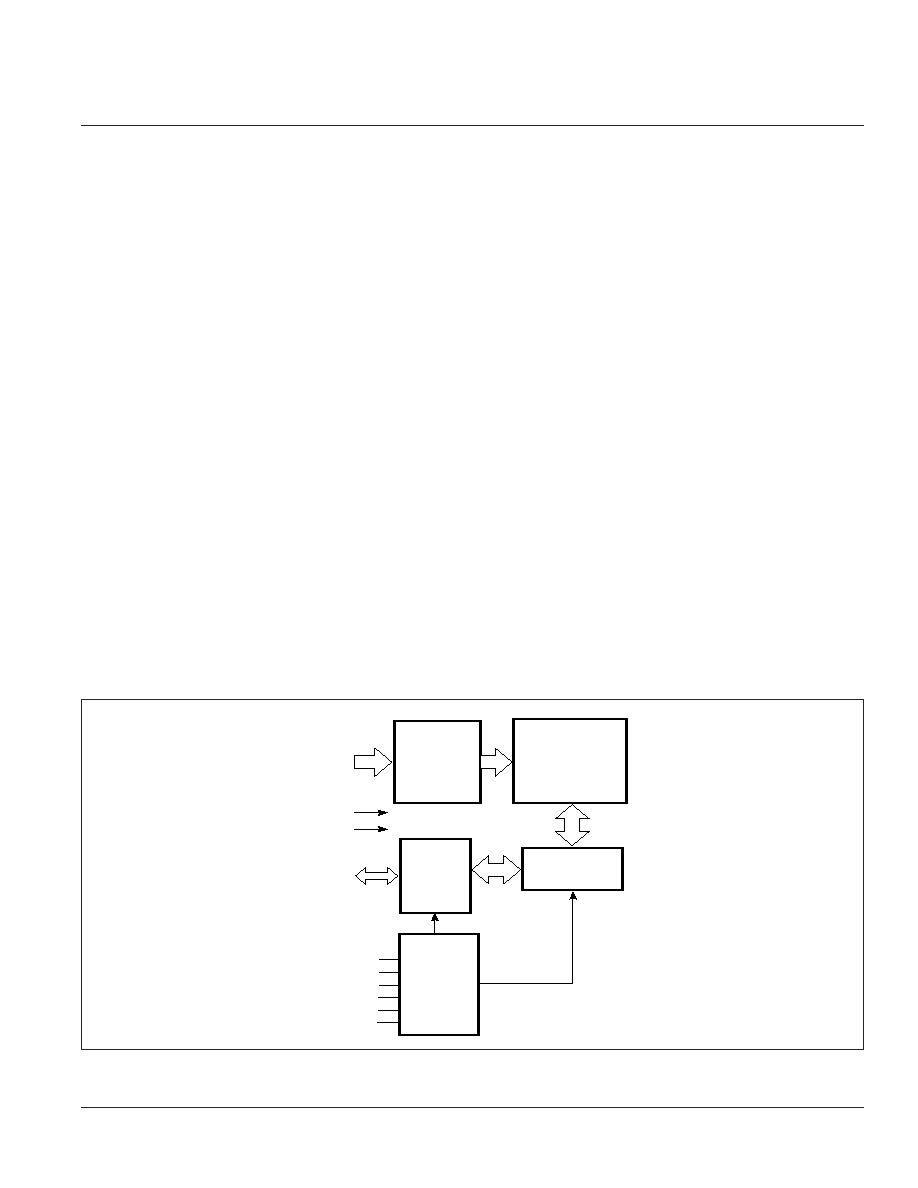
A0-A1
A2-A20/A21
LB
CS
WE
OE
1Mb x16
2Mb x 16
MEMORY ARRAY
DECODER
COLUMN I/O
CONTROL
CIRCUIT
GND
V
DD
I/O
DATA
CIRCUIT
CE
UB
I/O1-I/O16
FUNCTIONAL BLOCK DIAGRAM
IS32WV16100A/B
IS32WV16200A/B
ISSI
Æ
2
Integrated Silicon Solution, Inc. -- www.issi.com --
1-800-379-4774
Rev. 00B
01/20/03
PIN CONFIGURATIONS
PIN DESCRIPTIONS
A0-A21
Address Inputs
A0-A1
Page Address Inputs
I/O1 to I/O16 Data Input/Outputs
WE
Write Enable
OE
Output Enable
CE
Chip Enable Input
CS
Chip Select Input
LB, UB
Lower & Upper Data Byte Control Input
V
DD
Power
GND
Ground
NC
No Connection
IS32WV16100A/B (48-pin BGA)
1 2 3 4 5 6
A
B
C
D
E
F
G
H
A4
A17
UB
CS
A8
A12
A3
A7
LB
WE
A9
A13
A2
A6
A18
NC
A10
A14
A1
A5
NC
A19
A11
A15
A0
I/O
1
I/O
3
I/O
6
I/O
8
A16
CE
I/O
9
I/O
11
I/O
13
I/O
15
NC
OE
I/O
10
I/O
12
V
DD
I/O
14
I/O
16
GND
I/O
2
I/O
4
I/O
5
I/O
7
GND
1 2 3 4 5 6
A
B
C
D
E
F
G
H
A4
A17
UB
CS
A8
A12
A3
A7
LB
WE
A9
A13
A2
A6
A18
A20
A10
A14
A1
A5
NC
A19
A11
A15
A0
I/O
1
I/O
3
I/O
6
I/O
8
A16
CE
I/O
9
I/O
11
I/O
13
I/O
15
NC
OE
I/O
10
I/O
12
V
DD
I/O
14
I/O
16
GND
I/O
2
I/O
4
I/O
5
I/O
7
GND
IS32WV16200A/B (48-pin BGA)
IS32WV16100A/B
IS32WV16200A/B
ISSI
Æ
Integrated Silicon Solution, Inc. -- www.issi.com --
1-800-379-4774
3
Rev. 00B
01/20/03
TRUTH TABLE
Function
CE
CS
OE WE
LB
UB
ADD
I
/O1 to I/O8 I/O9 to I/O16 Power
Read: Word
L
H
L
H
L
L
XX
I/O
OUT
I/O
OUT
I
CC
1
Read: Lower Byte
L
H
L
H
L
H
XX
I/O
OUT
H
IGH
-Z
I
CC
1
Read: Upper Byte
L
H
L
H
H
L
XX
H
IGH
-Z
I/O
OUT
I
CC
1
Write: Word
L
H
X
L
L
L
XX
D
IN
D
IN
I
CC
1
Write: Lower
L
H
X
L
L
H
XX
D
IN
I
NVALID
I
CC
1
Write: Upper
L
H
X
L
H
L
XX
I
NVALID
D
IN
I
CC
1
Outputs Disabled
L
H
H
H
X
X
XX
H
IGH
-Z
H
IGH
-Z
I
SB
Standby
H
H
X
X
X
X
X
H
IGH
-Z
H
IGH
-Z
I
SB
Deep Power-Down Standby
H
L
X
X
X
X
X
H
IGH
-Z
H
IGH
-Z
I
SB
3
L = V
IL
, H =V
IH
, X = V
IL
or V
IH
, High-Z = High-impedence. XX = At
CE
falling edge, all addresses (A2 to A20) are valid "
IN
". Page
address signals (A0 and A1) must be V
IH
or V
IL
, during entire cycle.
IS32WV16100A/B
IS32WV16200A/B
ISSI
Æ
4
Integrated Silicon Solution, Inc. -- www.issi.com --
1-800-379-4774
Rev. 00B
01/20/03
ABSOLUTE MAXIMUM RATINGS
(1)
Symbol
Parameters
Rating
Unit
V
T
Voltage on Any Pin Relative to GND
≠0.2 to V
DD
+3.6
V
V
DD
Supply Voltage
≠0.2 to V
DD
+3.6
V
I
OUT
Output Current
50
mA
P
D
Power Dissipation
0.6
W
T
A
Commercial Operation Temperature
0 to +70
∞C
Industrial Temperature
≠40 to +85
∞C
T
STG
Storage Temperature
≠55 to +150
∞C
Note:
1. Stress greater than those listed under ABSOLUTE MAXIMUM RATINGS may cause permanent damage to the device. This is a
stress rating only and functional operation of the device at these or any other conditions above those indicated in the operational
sections of this specification is not implied. Exposure to absolute maximum rating conditions for extended periods may affect
reliability.
IS32WV16100A/IS32WV16200A
RECOMMENDED OPERATING CONDITIONS (Voltages are referenced to GND.)
Symbol
Parameter
Min.
Typ.
Max.
Unit
V
DD
Supply Voltage
1.65
2.2
V
V
IH
Input High Voltage
1.4
--
V
DD
+ 03
V
V
IL
Input Low Voltage
≠0.2
--
0.4
V
V
DH
Data Retention Supply Voltage
1.5
--
2.0
V
IS32WV16100B/IS32WV16200B
RECOMMENDED OPERATING CONDITIONS (Voltages are referenced to GND.)
Symbol
Parameter
Min.
Typ.
Max.
Unit
V
DD
Supply Voltage
2.2
3.6
V
V
IH
Input High Voltage
2.0
--
V
DD
+ 03
V
V
IL
Input Low Voltage
≠0.2
--
0.4
V
V
DH
Data Retention Supply Voltage
2.0
--
3.0
V
IS32WV16100A/B
IS32WV16200A/B
ISSI
Æ
Integrated Silicon Solution, Inc. -- www.issi.com --
1-800-379-4774
5
Rev. 00B
01/20/03
CAPACITANCE
(1,2)
Symbol
Parameter
Max.
Unit
C
IN
1
Input Capacitance: A0-A21
10
pF
C
IN
2
Input Capacitance:
CE,
CS,
OE, WE, LB, UB
10
pF
C
IO
Data Input/Output Capacitance: I/O0-I/O16
10
pF
Notes:
1. Tested initially and after any design or process changes that may affect these parameters.
2. Test conditions: T
A
= 25∞C, f = 1 MHz.
ELECTRICAL CHARACTERISTICS
(1)
(Recommended Operating Conditions unless otherwise noted.)
Symbol Parameter
Test Condition
Cond.
Min.
Max.
Unit
I
IL
Input Leakage Current
Any input 0V
V
IN
V
DD
≠1.0
1.0
µA
Other inputs not under test = 0V
I
IO
Output Leakage Current
Output is disabled (Hi-Z)
≠1.0
1.0
µA
0V
V
OUT
V
DD
V
OH
Output High Voltage Level
I
OH
= ≠0.5 mA
1.4
--
V
V
OL
Output Low Voltage Level
I
OL
= 1.0 mA
--
0.2
V
I
CC
1
Operating Current
CS
=V
IH
, I
OUT
= 0mA
32WV16100A/B --
20
mA
CE
Cycling, t
RC
= t
RC
(min.)
32WV16200A/B --
30
mA
I
CC
2
Page Access
CE
=V
IL
, CS=V
IH
, I
OUT
= 0mA
32WV16100A/B --
40
mA
Operating Currentt
Page Add.Cycling, t
PC
(min.)
32WV16200A/B --
5
mA
t
PC
>1
µ
A
I
SB
1
Standby Current: TTL
CE
=V
IH
,
CS=V
IH
32WV16100A/B --
1.5
mA
Commerical Temp
32WV16200A/B --
3
mA
Industrial Temp
CE
=V
IH
, CS= V
IH
32WV16100A/B --
3
mA
32WV16200A/B --
6
mA
I
SB
2
Standby Current: CMOS
CE
=Vss-0.2V, CS=V
DD
-0.2V
32WV16100A/B --
60
µA
Commercial Temp
32WV16200A/B --
70
µA
Industrial Temp
CE
=Vss-0.2V, CS=V
DD
-0.2V
32WV16100A/B --
70
µA
32WV16200A/B --
90
µA
I
SB
3
Standby Current:
CS
=0.2V
32WV16100A/B --
5
µA
Deep Power-down
32WV16200A/B --
5
µA
Commercial Temp
Industrial Temp
CS
=0.2V
32WV16100A/B --
10
µA
32WV16200A/B --
10
µA